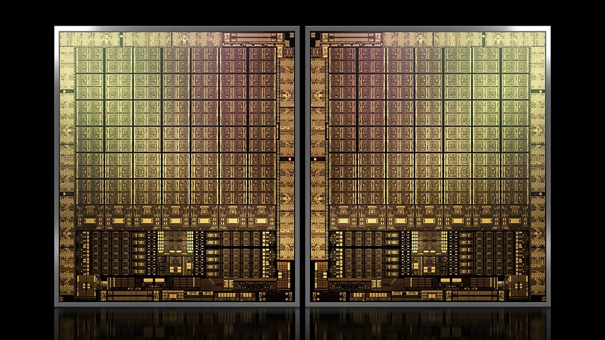
GH100, NVIDIA's next-generation data center "Hopper" GPU, according to recent rumors from Chip Hell, will have some truly mind-blowing specs, according to the publication.
As claimed by user zhangzhonghao, the transistor count of this GPU will be 140 billion, an astounding number that exceeds current flagship data center GPUs such as AMD's Aldebaran (58.2 billion transistors) and NVIDIA's GA100 (58.2 billion transistors), respectively (54.2 billion transistors). In prior reports, it was stated that NVIDIA's GH100 would be manufactured utilizing 5-nanometer technology and would have a die size of close to 1000 mm2, making it the world's largest graphics processing unit.
Furthermore, according to reports, Nvidia has developed what is called the COPA solution, based on the Hopper architecture. A COPA-GPU is a domain-specialized composable GPU architecture capable to provide high levels of GPU design reuse across the #HPC and #DeepLearning domains, while enabling specifically optimized products for each domain. With two separate designs based on the same architecture, Nvidia will supply two distinct solutions: one for high-performance computing (HPC) and another for deep learning (DL). While HPC will use the standard technique, DL will make use of a vast independent cache that will be coupled to the graphics processor.
Nvidia is expected to unveil the Hopper architecture GPU at GTC 2022, where it will be detailed.
140 billion transistors for Nvidia Hopper GH100 GPU?