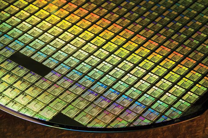
There's always something smaller. TSMC announced its 6-nanometer (N6) process, which provides a enhancement of its 7nm technology and offers customers a competitive performance-to-cost advantage as well as fast time-to-market with direct migration from N7-based designs.
By leveraging the new capabilities in extreme ultraviolet (EUV) lithography gained from the N7+ technology currently in risk production, TSMC’s N6 process delivers 18% higher logic density over the N7 process. At the same time, its design rules are fully compatible with TSMC’s proven N7 technology, allowing its comprehensive design ecosystem to be reused. As a result, it offers a seamless migration path with a fast design cycle time with very limited engineering resources for customers to achieve the product benefits from the new technology offering.
Scheduled for risk production in the first quarter of 2020, TSMC’s N6 technology provides customers with additional cost-effective benefits while extending the industry-leading power and performance from the 7nm family for a broad array of applications, ranging from high-to-mid end mobile, consumer applications, AI, networking, 5G infrastructure, GPU, and high-performance computing.
“TSMC N6 technology will further extend our leadership in delivering product benefits with higher performance and cost advantage beyond the current N7,” said Dr. Kevin Zhang, TSMC Vice President of Business Development. “Building upon the broad success of our 7nm technology, we’re confident that our customers will be able to quickly extract even higher product value from the new offering by leveraging a well-established design ecosystem today.”