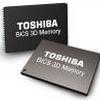
Toshiba unveiled the new generation of BiCS FLASH, a three-dimensional (3D) stacked cell structure flash memory. The new device is the world's first 256-gigabit (32gigabytes) 48-layer BiCS device and also deploys industry-leading 3-bit-per-cell (triple-level cell, TLC) technology.
BiCS FLASH is based on a leading-edge 48-layer stacking process that surpasses the capacity of mainstream two dimensional NAND Flash memory while enhancing write/erase reliability endurance and boosting write speeds. The new 256 Gb device is suited for diverse applications, including consumer SSD, smartphones, tablets and memory cards, and enterprise SSD for data centers.
Toshiba has a long-standing commitment to flash memory, and is currently readying for mass production of BiCS FLASH in a new Fab2 at Yokkaichi Operations, its production site for NAND flash memories. Fab2 will be completed in the first half of 2016.

