It's always interesting to see a chip up-close and personal. As you all know. AMD has been behind the one empowering the new Xbox and PlayStation 5, that last for that last one pictures emerged.
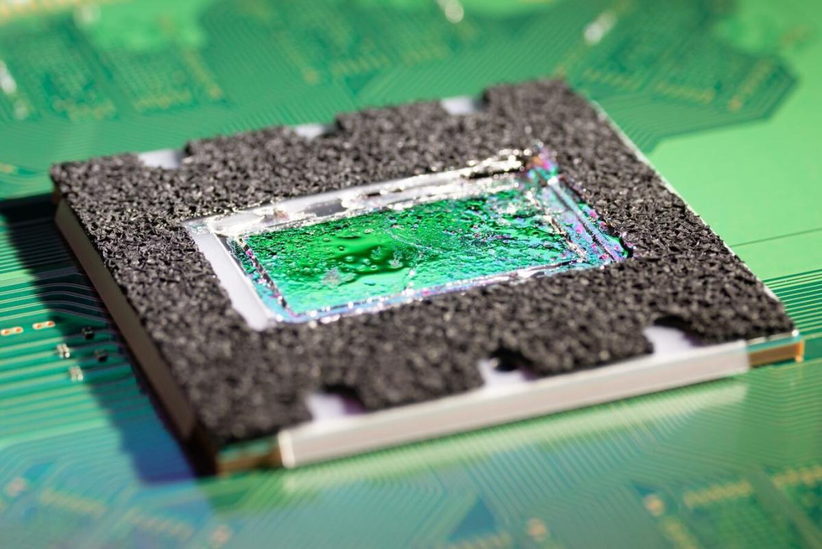
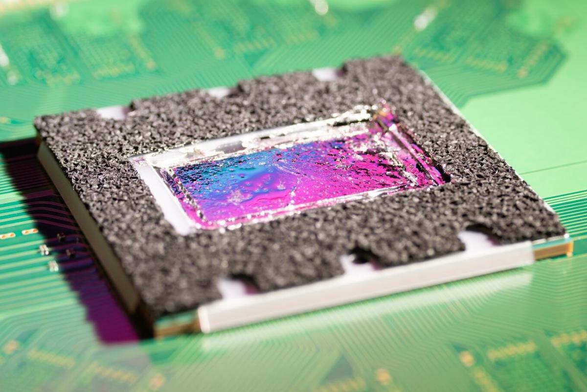
Microsoft shared a photo of the AMD-soc in the Series X long before the release, Sony remained a bit quieter in that regard. Chip photographer Fritzchens Fritz has now changed that, by shooting a few relatively detailed pictures of the silicon in the Playstation 5.Based on AMD Zen2 cores reaching up to 3.5 GHz, the CPU is matched with 36 shading core clusters based on RDNA 2 running up to 2.23 GHz. Inbetween heatsink and processor liquid metal is present. Surrounding the die you can see some conductive material used, likely to keep that liquid metal in place. Firing off Using a special short wave infrared light (SWIR) microscope shows the CPU core complex and a GPU area. Now, there appear to be 40 CU's physically on the die, which would mean that Sony is not using four. This could have been done from a yield point of view.
Fritzchens Fritz: A first quick and dirty die-shot of the PS5 APU (better SWIR image will follow). It looks like some Zen 2 FPU parts are missing.
Locuza: My interpretation of the floor plan PS5 floor plan: 1. Bomba surprise that Sony likely cut down the 256-Bit FP pipes to just 128-Bit. 2. No Infinity Cache/L3$, also not on the Xbox Series. 3. Might have the old Render Backend design, need higher res to say for sure. 4. ...
Sources: Fritzchens Fritz, Locuza, via VideoCardz