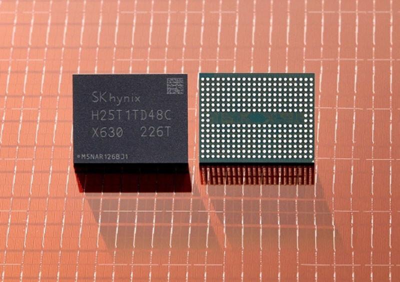
The company's latest prototype boasts over 300 layers, a significant improvement over its previous record holding seventh-generation 238-layer 3D NAND. A team of 35 engineers prepared the presentation.
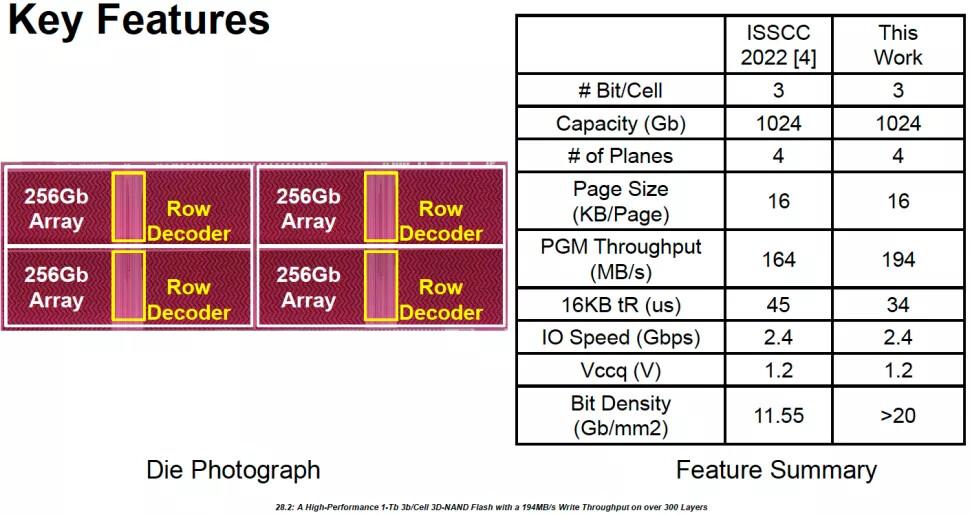
The eighth-generation 3D NAND offers an 18% increase in performance compared to the older model, with a maximum bandwidth of 194 MB/s. This advancement is expected to provide faster processing and data transfer speeds, benefiting end consumers. Additionally, the new chip's 300+ active layer design provides a high recording density of over 20 GB/mm^2, enabling a capacity of 1 TB (128 GB) with triple level cells. The chip features a 16 KB page size, four planes and a 2400 MT/s interface. The increased density will result in a lower cost per TB during the manufacturing process. SK Hynix's latest breakthrough in 3D NAND technology is set to revolutionize the semiconductor industry, and it is hoped that the end consumers will ultimately benefit from the boost in performance and capacity.Five areas of technological implementations for the eighth-generation 3D NAND have been identified:
- Triple-Verify Program (TPGM) feature that narrows cell threshold voltage distribution and reduces tPROG (program time) by 10%, which translates into higher performance
- Adaptive Unselected String Pre-Charge (AUSP) - another procedure to reduce tPROG by around 2%
- All-Pass Rising (APR) scheme that reduces tR (read time) by approximately 2% and cuts word line rising time
- Programmed Dummy String (PDS) technique that cuts world line settling time for tPROG and tR by reducing channel capacitance load
- Plane-Level Read Retry (PLRR) capability that allows to change read level of a plane without terminating others therefore issuing subsequent read commands immediately and improving quality of service (QoS) and therefore read performance
Although the company has not disclosed a specific timeline for production, industry experts believe that development is either completed or near completion. Typically, flash memory manufacturers tend to slow down the adoption of new manufacturing nodes to manage NAND bit output, suggesting that SK Hynix is unlikely to rush 8th Gen 3D NAND to production. Instead, it is reasonable to expect that this groundbreaking technology will be adopted in 2024.
SK Hynix reveals 300-layer 3D NAND prototype with improved performance and recording density