SK Hynix is showing details on their first DDR5 chip. The standard is officially still under development by Jedec, but seems to make an appearance soon enough..
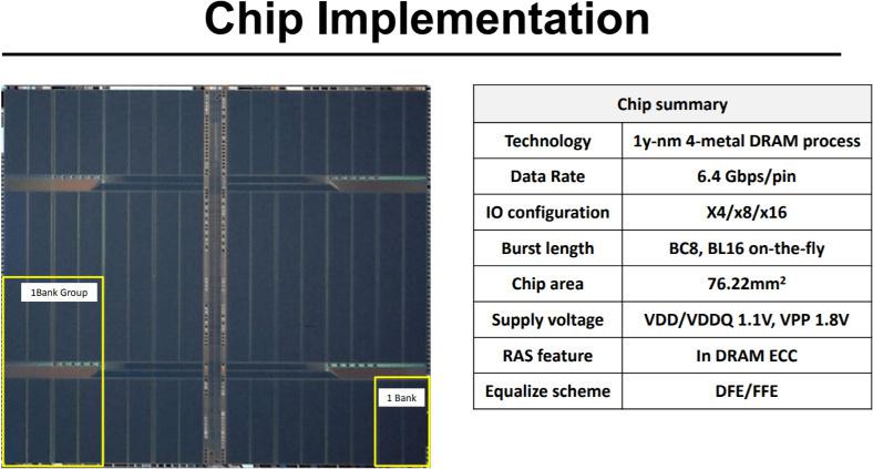
DDR5 — or Double Data Rate 5 — is still under development at the Jedec standards organization. DDR5 offers double the bandwidth and double the density of DDR4 along with delivering improved channel efficiency. The standard was expected to be finalized last year, but remains a work in progress. DDR5 products are now expected to appear beginning late this year report eetimes. Dongkyun Kim, a Hynix chip designer, presented the ISSCC paper Wednesday on the Hynix DDR5 chip, a 16Gb 6.4Gb/s/pin SDRAM that runs at 1.1V and measures 76.22mm2. The device is fabricated in a 1ynm, 4-metal DRAM process.
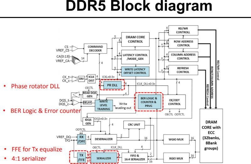
Kim described the implementation of a modified delay-locked loop (DLL) using a phase rotator and an injection locked oscillator to reduce clock jitter and clock duty cycle distortion associated with operating at higher clock speeds. He also described other techniques used by the Hynix design team, including a write-level training method to offset clock-domain issues associated with higher speeds and a modified forward feedback equalization (FFE) circuit.
Samsung, meanwhile, described a 10nm-class LPDDR5 SDRAM capable of up to 7.5Gb/s at 1.05V.
Jedec announced earlier this week the publication of the LPDDR5 standard, which will eventually operate at an I/O rate of 6400 MT/s, 50% higher than that of the first version of LPDDR4. It is expected to boost memory speed and efficiency for applications including smartphones, tablets and ultra-thin notebooks.
SK Hynix publishes details first DDR5 chip