Samsung’s 3nm Gate-All-Around (GAA) process, 3GAE, development is on track. The company noted today that its Process Design Kit (PDK) version 0.1 for 3GAE has been released in April to help customers get an early start on the design work and enable improved design competitiveness along with reduced turnaround time (TAT).
Compared to 7nm technology, Samsung’s 3GAE process is designed to provide up to a 45 percent reduction in chip area with 50 percent lower power consumption or 35 percent higher performance. The GAA-based process node is expected to be widely adopted in next-generation applications, such as mobile, network, automotive, Artificial Intelligence (AI) and IoT.
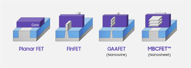
Conventional GAA based on nanowire requires a larger number of stacks due to its small effective channel width. On the other hand, Samsung’s patented version of GAA, MBCFET™ (Multi-Bridge-Channel FET), uses a nanosheet architecture, enabling greater current per stack.
While FinFET structures must modulate the number of fins in a discrete way, MBCFET™ provides greater design flexibility by controlling the nanosheet width. In addition, MBCFET™’s compatibility with FinFET processes means the two can share the same manufacturing technology and equipment, which accelerates process development and production ramp-up. Samsung recently taped out the 3GAE test vehicle design and will focus on improving its performance and power efficiency going forward.
Process technology roadmap and advanced packaging updates
Samsung’s roadmap includes four FinFET-based processes from 7nm down to 4nm that leverage extreme ultraviolet (EUV) technology as well as 3nm GAA, or MBCFET™.
In the second half of this year, Samsung is scheduled to start the mass production of 6nm process devices and complete the development of 4nm process. The product design of Samsung’s 5nm FinFET process, which was developed in April, is expected to be completed in the second half of this year and go under mass production in the first half of 2020.
Extensions of the company’s FD-SOI (FDS) process and eMRAM together with an expanded set of state-of-the-art package solutions were also unveiled at this year’s Foundry Forum. Development of the successor to the 28FDS process, 18FDS, and eMRAM with 1Gb capacity will be finished this year.
You can check an infographic here.