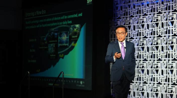
Samsung announced a comprehensive foundry process technology roadmap to 8nm, 7nm, 6nm, 5nm, 4nm and 18nm FD-SOI in its newest process technology roadmap.
“The ubiquitous nature of smart, connected machines and everyday consumer devices signals the beginning of the next industrial revolution,” said Jong Shik Yoon, Executive Vice President of the Foundry Business at Samsung Electronics. “To successfully compete in today’s fast-paced business environment, our customers need a foundry partner with a comprehensive roadmap at the advanced process nodes to achieve their business goals and objectives.”
Samsung’s newest foundry process technologies and solutions introduced at the annual Samsung Foundry Forum include:
- 8LPP (8nm Low Power Plus): 8LPP provides the most competitive scaling benefit before transitioning to EUV (Extreme Ultra Violet) lithography. Combining key process innovations from Samsung’s 10nm technology, 8LPP offers additional benefits in the areas of performance and gate density as compared to 10LPP.
- 7LPP (7nm Low Power Plus): 7LPP will be the first semiconductor process technology to use an EUV lithography solution. 250W of maximum EUV source power, which is the most important milestone for EUV insertion into high volume production, was developed by the collaborative efforts of Samsung and ASML. EUV lithography deployment will break the barriers of Moore’s law scaling, paving the way for single nanometer semiconductor technology generations.
- 6LPP (6nm Low Power Plus): 6LPP will adopt Samsung’s unique Smart Scaling solutions, which will be incorporated on top of the EUV-based 7LPP technology, allowing for greater area scaling and ultra-low power benefits.
- 5LPP (5nm Low Power Plus): 5LPP extends the physical scaling limit of FinFET structure by implementing technology innovations from the next process generation, 4LPP, for better scaling and power reduction.
- 4LPP (4nm Low Power Plus): 4LPP will be the first implementation of next generation device architecture – MBCFETTM structure (Multi Bridge Channel FET). MBCFETTM is Samsung’s unique GAAFET (Gate All Around FET) technology that uses a Nanosheet device to overcome the physical scaling and performance limitations of the FinFET architecture.
- FD-SOI (Fully Depleted – Silicon on Insulator): Well suited for IoT applications, Samsung will gradually expand its 28FDS technology into a broader platform offering by incorporating RF (Radio Frequency) and eMRAM(embedded Magnetic Random Access Memory) options. 18FDS is the next generation node on Samsung’s FD-SOI roadmap with enhanced PPA (Power/Performance/Area).
- EVP Yoon concluded that “Samsung Foundry’s advanced process technology roadmap is a testament to the collaborative nature of our customer and ecosystem partner relationships. The inclusion of the process technologies above will enable an explosion of new devices that will connect consumers in ways never seen before.”
Samsung Talks Future of Foundry with Process Roadmap Down to 4nm


