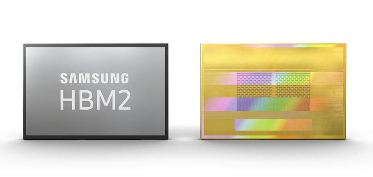
Samsung announced that it has started mass production of its 2nd-generation 8-gigabyte (GB) High Bandwidth Memory-2 (HBM2) with the fastest data transmission speed on the market today.
The new solution, Aquabolt, which is the industry's first HBM2 to deliver a 2.4 gigabits-per-second (Gbps) data transfer speed per pin, should accelerate the expansion of supercomputing and the graphics card market. "With our production of the first 2.4 Gbps 8 GB HBM2, we are further strengthening our technology leadership and market competitiveness," said Jaesoo Han, executive vice president, Memory Sales & Marketing team at Samsung Electronics. "We will continue to reinforce our command of the DRAM market by assuring a stable supply of HBM2 worldwide, in accordance with the timing of anticipated next-generation system launches by our customers."
Samsung's new 8GB HBM2 delivers the highest level of DRAM performance, featuring a 2.4 Gbps pin speed at 1.2V, which translates into a performance upgrade of nearly 50 percent per each package, compared to the company's 1st-generation 8 GB HBM2 package with its 1.6 Gbps pin speed at 1.2V and 2.0 Gbps at 1.35V.
With these improvements, a single Samsung 8GB HBM2 package will offer a 307 gigabytes-per-second (GBps) data bandwidth, achieving 9.6 times faster data transmission than an 8 gigabit (Gb) GDDR5 chip, which provides a 32 GBps data bandwidth. Using four of the new HBM2 packages in a system will enable a 1.2 terabytes-per-second (TB/s) bandwidth., which will improve overall system performance by as much as 50 percent, compared to a system that uses a 1.6 Gbps HBM2.
Samsung's new Aquabolt significantly extends the company's leadership in driving the growth of the premium DRAM market. Moreover, Samsung will continue to offer leading-edge HBM2 solutions, to succeed its 1st-generation HBM2, Flarebolt, and its 2nd-generation, Aquabolt, as it further expands the market over the next several years.
To achieve Aquabolt's unprecedented performance, Samsung has applied new technologies related to TSV design and thermal control. A single 8GB HBM2 package consists of eight 8Gb HBM2 dies, which are vertically interconnected using over 5,000 TSVs (Through Silicon Via's) per die. While using so many TSVs can cause collateral clock skew, Samsung succeeded in minimizing the skew to a very modest level and significantly enhancing chip performance in the process.
In addition, Samsung increased the number of thermal bumps between the HBM2 dies, which enables stronger thermal control in each package. Also, the new HBM2 includes an additional protective layer at the bottom, which increases the package's overall physical strength.
In accommodating the growing need for high-performance HBM2 DRAM, Samsung will supply Aquabolt to its global IT customers at a stable pace, and continue to rapidly advance its memory technology in conjunction with leading OEMs throughout a wide array of fields including supercomputing, artificial intelligence, and graphics processing.