Samsung and Qualcomm Working on 7nm EUV Process Technology
Samsung announced the intention to expand their decade-long foundry relationship into EUV (extreme ultra violet) lithography process technology, including the manufacture of future Qualcomm Snapdragon 5G mobile chipsets using Samsung’s 7-nanometer (nm) LPP (Low Power Plus) EUV process technology.
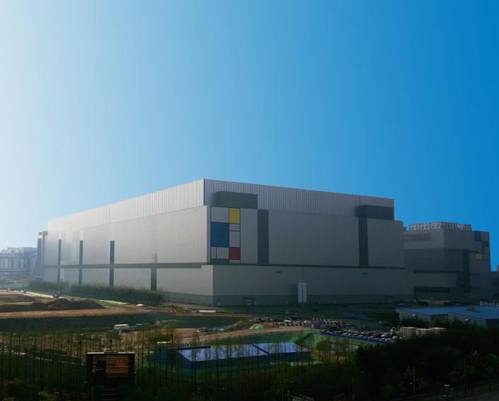
Qualcomm anticipates that its future Snapdragon 5G mobile chipsets will use Samsung’s 7nm LPP EUV process technology. Using 7LPP EUV process technology, Snapdragon 5G mobile chipsets will offer a smaller chip footprint, giving OEMs more usable space inside upcoming products to support larger batteries or slimmer designs. Process improvements, combined with a more advanced chip design, are expected to bring significant improvements in battery life. Last May, Samsung introduced 7LPP EUV, its first semiconductor process technology to use an EUV lithography solution. It is anticipated that EUV lithography deployment will break the barriers of Moore’s law scaling, paving the way for single nanometer semiconductor technology generations.
Compared with its 10nm FinFET predecessors, Samsung’s 7LPP EUV technology not only greatly reduces the process complexity with fewer process steps and better yield, but also allows up to a 40 percent increase in area efficiency with 10 percent higher performance or up to 35 percent lower power consumption.
“We are excited to lead the 5G mobile industry together with Samsung,” said RK Chunduru, senior vice president, supply chain and procurement, Qualcomm Technologies, Inc. “Using 7nm LPP EUV, our new generation of Snapdragon 5G mobile chipsets will take advantage of the process improvements and advanced chip design to improve the user experience of future devices.”
“We are pleased to continue to expand our foundry relationship with Qualcomm Technologies in 5G technologies using our EUV process technology,” said Charlie Bae, Executive Vice President of Foundry Sales and Marketing Team at Samsung Electronics. “This collaboration is an important milestone for our foundry business as it signifies confidence in Samsung’s leading process technology.”
Samsung Working on OLED TVs based on Blue OLEDs and quantum dots - 02/22/2018 10:11 AM
Will it finally happen, Samsung supposedly has been showing prototypes of OLED TVs in of 55 "and 65" sizes. The new prototypes OLED screens would use blue OLEDs with red and green color f...
Samsung Starts Volume Production of a 30.72-terabyte SSD - 02/20/2018 09:38 AM
And before you get your hopes up, you'll never be able to afford it :) Samsung announced that it has begun mass producing the industry's largest capacity Serial Attached SCSI (SAS) solid state driv...
Samsung has surplus OLED screens due to disappointing iPhone X sales - 02/19/2018 10:09 AM
It's a bit of a paradox when you think about it, but Samsung has a surplus of OLED displays, because sales of the iPhone X are not at the level they should be....
Samsung Halts Galaxy S8 Oreo Update Due to Reboot Bug - 02/16/2018 09:57 AM
Samsung has halted the Android 8 Oreo update for the Galaxy S8 after users reported random reboots. "Following a limited number of cases where Galaxy S8 and S8+ devices have rebooted unexpectedl...
Samsung Mass Production of 256GB Embedded Flash Storage for Automotive - 02/08/2018 10:42 AM
Samsung Electronics, the world leader in advanced memory technology, today announced that it has begun mass production of a 256-gigabyte (GB) embedded Universal Flash Storage (eUFS) solution with adva...
Senior Member
Posts: 11808
Joined: 2012-07-20
Very interesting times. It's really hard to comprehend how 20 years ago transistors were ~35x bigger.
I personally think I'll be avoiding sub-7nm products for a little while, until I hear more about reliability and data integrity. Engineers might be able to work around the limitations of physics, but you can't cheat or change physics.
They'll never put it into production unless it has certain level of reliability. As recall of millions of chips from very expensive devices may put foundry under.
Till now we have not seen any significant chip degradation over time. Biggest problem is to get defect-less chip. And they seem to be overcoming it.
Senior Member
Posts: 7434
Joined: 2012-11-10
EDIT:
Nevermind
Senior Member
Posts: 11808
Joined: 2012-07-20
Yes, but if they go for mass production, they trust it. Maybe High clock OC may become issue. But on other hand, those devices will be 1st in lower clock, high efficiency phones, tablets

Senior Member
Posts: 7434
Joined: 2012-11-10

I just realized that these don't appear to be traditional silicon-based transistors, and were in development for years along side traditional transistors. So - I'm pretty sure I'm wrong about what I was thinking anyway.
Senior Member
Posts: 7434
Joined: 2012-11-10
Very interesting times. It's really hard to comprehend how 20 years ago transistors were ~35x bigger.
I personally think I'll be avoiding sub-7nm products for a little while, until I hear more about reliability and data integrity. Engineers might be able to work around the limitations of physics, but you can't cheat or change physics.