Samsung shared new details on it's upcoming NAND flash memories, which would include the 8th generation of V-NAND, discussing up-to the 10th generation type products. And yes Samsung will go after QLC (4-bits per cell) based NAND flash as well.
QLC has certain advantaged and disadvantages. The advantage of course is the ability to create more volume with less cells. Samsung has been talking a (you are reading it right) a 128 terabyte SAS SSD. V-NAND V4 was 64-layer TLC, V5 is a move to QLC, bringing per die capacity to 1Tbit (128 GB per die). The unit would get die NAND sizes of 1 TB and Samsung mentions 32 die's per package as reported at Tomshardware.
QLC-NAND is based upon 64-layer stacked NAND cells that can produce a capacity of 768 gigabit, allowing for 1.5 TB of storage per package. That means this type of NAND will bring high volume SSDs in vicinity, availability while remaining very cost-effective. Basically this type of NAND thus writes 4 bits per cell. Adding more bits per cell also has an effect on the life-span of the NAND cell, and thus that brings down the number of times it can be written. Much like TLC (Triple level cell) many new technologies like error-correction mechanisms and wearing have increased the life-span of the respective SSDs. For example a 500 GB TLC based SSD can quite easily manage a 300TB written before NAND cells start to die off. TLC has roughly a 1000 PE cycles, that is lower for QLC. However, the competition (Toshiba) already managed to achieve a 1000 P/E cycles.
It will not be a fast SSD though as QLC is slower than TLC, but with so many channels something probably will compensate for that somewhere.
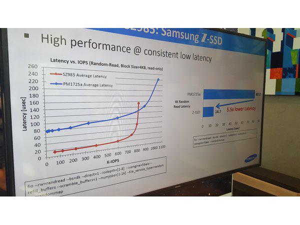
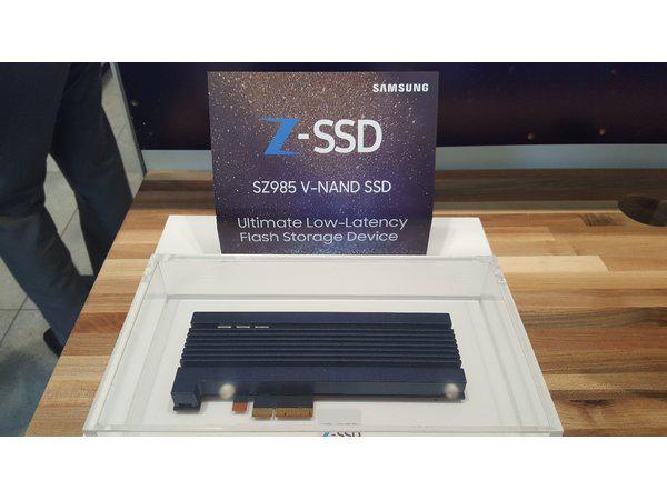
Samsung also talked about Z-NAND, the competition for intel Optane. It's based on an optimized SLC-flash (Single-level cell). The first ones are already sampled to customers and the product is named SZ985.
QLC however, that'll be a while.
--- Press release
August 8, 2017 – Samsung Electronics Co., Ltd., the world leader in advanced memory technology, has announced new V-NAND (Vertical NAND) memory solutions and technology that will address the pressing requirements of next-generation data processing and storage systems. With the rapid increase of data-intensive applications across many industries using artificial intelligence and Internet of Things (IoT) technologies, the role of flash memory has become extremely critical in accelerating the speed at which information can be extracted for real-time analysis. At the inaugural Samsung Tech Day* and this year’s Flash Memory Summit**, Samsung is showcasing solutions to address next-generation data processing challenges centered around the company’s latest V-NAND technology and an array of solid state drives (SSDs). These solutions will be at the forefront of enabling today’s most data-intensive tasks such as high-performance computing, machine learning, real-time analytics and parallel computing. “Our new, highly advanced V-NAND technologies will offer smarter solutions for greater value by providing high data processing speeds, increased system scalability and ultra-low latency for today’s most demanding cloud-based applications,” said Gyoyoung Jin, executive vice president and head of Memory Business at Samsung Electronics. “We will continue to pioneer flash innovation by leveraging our expertise in advanced 3D-NAND memory technology to significantly enhance the way in which information-rich data is processed. Samsung heralds era of 1-terabit (Tb) V-NAND chip Samsung announced a 1Tb V-NAND chip that it expects to be available next year.
Initially mentioned in 2013, during unveiling of the industry’s first 3D NAND, Samsung has been working to enable its core memory technologies to realize one terabit of capacity on a single chip using a V-NAND structure. The arrival of a 1Tb V-NAND chip next year will enable 2TB of memory in a single V-NAND package by stacking 16 1Tb dies and will represent one of the most important memory advances of the past decade. NGSFF (Next Generation Small Form Factor) SSD to improve server storage capacity and IOPS Samsung is sampling the industry’s first 16-terabyte (TB) NGSFF SSD, which will dramatically improve the memory storage capacity and IOPS (input/output operations per second) of today’s 1U rack servers. Measuring 30.5mm x 110mm x 4.38mm, the Samsung NGSFF SSD provides hyper-scale data center servers with substantially improved space utilization and scaling options. Utilizing the new NGSFF drive instead of M.2 drives in a 1U server can increase the storage capacity of the system by four times. To highlight the advantages, Samsung demonstrated a reference server system that delivers 576TB in a 1U rack, using 36 16TB NGSFF SSDs.
The 1U reference system can process about 10 million random read IOPS, which triples the IOPS performance of a 1U server equipped with 2.5-inch SSDs. A petabyte capacity can be achieved using only two of the 576TB systems. Samsung plans to begin mass producing its first NGSFF SSDs in the fourth quarter of this year, while working to standardize the form factor with industry partners. Z-SSD: optimized for systems requiring fast memory responsiveness Following last year’s introduction of its Z-SSD technology, Samsung introduced its first Z-SSD product, the SZ985. Featuring ultra-low latency and high performance, the Z-SSD will be used in data centers and enterprise systems dealing with extremely large, data-intensive tasks such as real-time “big data” analytics and high-performance server caching. Samsung is collaborating with several of its customers on integrating the Z-SSD in upcoming applications. The Samsung SZ985 requires only 15 microseconds of read latency time which is approximately a seventh of the read latency of an NVMe*** SSD. At the application level, the use of Samsung’s Z-SSDs can reduce system response time by up to 12 times, compared to using NVMe SSDs. With its fast response time, the new Z-SSD will play a pivotal role in eliminating storage bottlenecks in the enterprise and in improving the total cost of ownership (TCO). New approach to storage with proprietary Key Value SSD technology Samsung also introduced a completely new technology called Key Value SSD. The name refers to a highly innovative method of processing complex data sets. With the sharply increasing use of social media services and IoT applications, which contribute to the creation of object data such as text, image, audio and video files, the complexity in processing this data increases substantially. Today, SSDs convert object data of widely ranging sizes into data fragments of a specific size called "blocks.”
The use of these blocks requires implementation processes consisting of LBA (logical block addressing) and PBA (physical block addressing) steps. However, Samsung’s new Key Value SSD technology allows SSDs to process data without converting it into blocks. Samsung’s Key Value instead assigns a ‘key’ or specific location to each ”value,” or piece of object data – regardless of its size. The key enables direct addressing of a data location, which in turn enables the storage to be scaled. Samsung’s Key Value technology enables SSDs to scale-up (vertically) and scale-out (horizontally) in performance and capacity. As a result, when data is read or written, a Key Value SSD can reduce redundant steps, which leads to faster data inputs and outputs, as well as increasing TCO and significantly extending the life of an SSD.
Samsung Talks QLC and talks 128 terabyte SAS SSD