Radeon RX 570 and 580 Smile On Camera
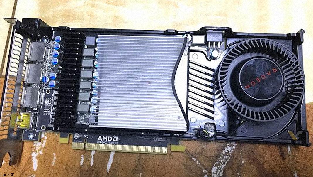
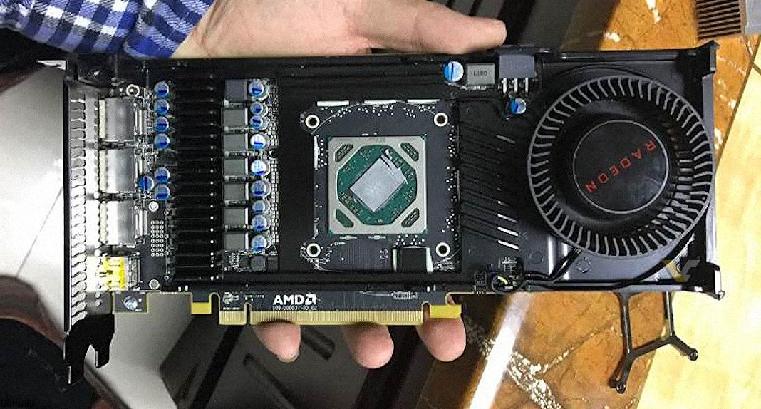
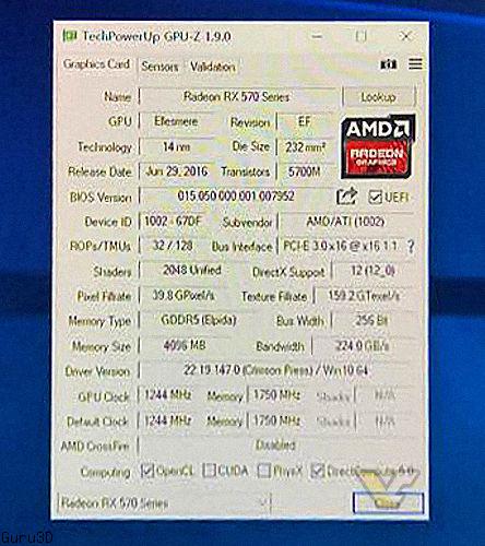
Photos of the Radeon RX 570 and 580 leaked on the web. There even is a GPU-Z screenshot displaying specs. It seems, the RX 570 will make use if the same PCB as Radeon RX 480/470 series.
Radeon RX 570
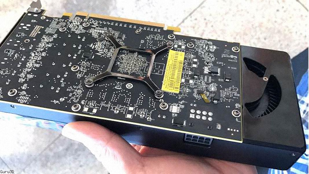
This board once again comes with a 6-pin power connector and your three DP and one HDMI connectors. This reference design again misses a DVI port. If the photos are for real then it confirms that Radeon RX 570 is using Polaris GPUs.
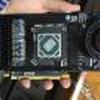
AMD Radeon RX 580
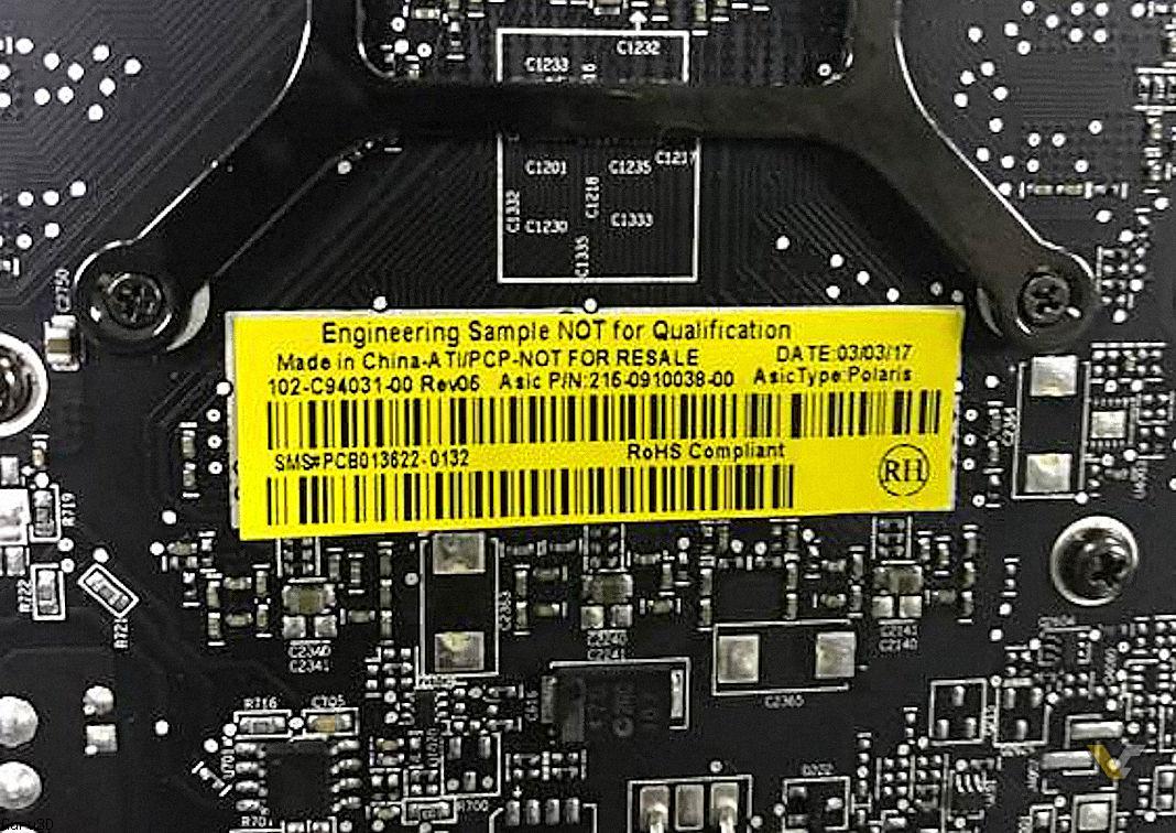
Pictures of Radeon RX 580 also have surfaced, including an engineering sample with board number C940. This graphics cards definitely seems to be new. The cards will get a 8-pin power connector. The label shows again, Polaris being fabbed March 3rd. For the specifications, a GPU-Z screenshot was also posted and it seems that the specs for RX 570 are 2048 Stream Processors, 128 TMUs and 32 ROPs. That's similar towards the Radeon RX 470s. If the screenshot is for real, the AMD has not increased the memory speed on new Polaris SKUs. The RX 570 4GB will have 4GB and 8GB GDDR5 memory configurations at 7 GHz effective frequency. The Radeon RX 500 series are rumored to launch on April 18th. For the RX 580, there is still shatter on the web about special XTR version (normally you have Pro and XT codes, now a XTR code was spotted), a higher clocked version of the product series that could make a difference. We'll see.
Radeon RX 580 | Radeon RX 480 | Radeon RX 570 | Radeon RX 470 | |
---|---|---|---|---|
GPU | Polaris 10 | Polaris 10 | Polaris 10 | Polaris 10 |
Cores |
2304
|
2304
|
2048
|
2048
|
TMUs |
144
|
144
|
128
|
128
|
ROPs |
32
|
32
|
32
|
32
|
FP32 Compute |
6.17 TFLOPS
|
5.83 TFLOPS
|
5.10 TFLOPS
|
4.94 TFLOPS
|
Boost Clock |
~1340 MHz
|
1266 MHz
|
~1244 MHz
|
1206 MHz
|
Memory Clock |
8000 MHz
|
8000 MHz
|
7000 MHz
|
6600 MHz
|
Memory |
up to 8 GB
|
up to 8 GB
|
up to 8 GB
|
up to 8 GB
|
Memory Bus |
256-bit
|
256-bit
|
256-bit
|
256-bit
|
Bandwidth |
256 GB/s
|
256 GB/s
|
224 GB/s
|
211 GB/s
|
Memory Type | GDDR5 | GDDR5 | GDDR5 | GDDR5 |
Power Connector | 1x 8-pin | 1x 6-pin | 1x 6-pin | 1x 6-pin |
Radeon RX 500 Series fabbed using newer 14nm LPP - 03/20/2017 04:15 PM
We talked about the upcomign respin fromA MD quite a bit already. it seems that the GPUs however might get a slight advantage as AMD seems to be moving towards a LLP (low power plus) fabrication proce...
Radeon RX 560, 570 and 580 make an appearance in Crimson 17.3.2 driver - 03/16/2017 06:32 PM
AMD yesterday released Radeon Software Crimson ReLive 17.3.2 driver (download them here), and they offer support for the Radeon RX 580, RX 570 and 560....
Retail Design Radeon RX VEGA caught on camera? - 03/16/2017 06:18 PM
AMD has been hosting a technology summit in Beijing, China and Lisa Su made the official introduction of Ryzen 5 process family. From that event some weird screen grabs have been made. It could be a r...
AMD Unveils naming on VEGA - Radeon RX VEGA - 02/28/2017 09:55 PM
Right, this news-item will be as short as the announcement. AMD shared the final naming for the enthusiast card that we all know as VEGA. At GDC Raja Koduri announced the official brand name....
XFX adds Radeon RX 480 Crimson Edition to Lineup - 02/27/2017 11:07 AM
Yeah correct, that's names just like the AMD drivers. XFX seems to try and lift sales upon the brand recognition from AMD. The card is the Radeon RX 480 Crimson Edition 8 GB graphics located under S...
Senior Member
Posts: 859
Joined: 2017-02-17
So basically a rebrand? maybe a die shrink with a bump of the core clocks. Hopefully vega and big vega will help out AMD's top end line
Member
Posts: 40
Joined: 2016-07-27
What's the Point
I have an MSI RX-480 Gaming X 8G that does 1380/2100 all day long, and never exceeds 70°.
So, what's the point in these cards???
If you want one, find yourself a good deal on a 480, and overclock to the 580 specifications, or more.
Senior Member
Posts: 8199
Joined: 2010-11-16
I have an MSI RX-480 Gaming X 8G that does 1380/2100 all day long, and never exceeds 70°.
So, what's the point in these cards???
1. Because OEMs (oh and GPU partners too)
2. PCIe power delivery fix
3. Possible process refinement(not shrink) which brings yadayada
Senior Member
Posts: 2159
Joined: 2007-01-16
Die shrink(possibly) with slightly faster core clocks..
More re-branding just confuses general population..
Also I'm tired of seeing PEG connectors flat in the middle on top of GPU.
Put it on the side.
Top PEG just ruins those trying to perfect cable management.
Top PEG placement has been preferred since before, PEG connectors where they were placed at the end often ran into issues of getting in the way of 2.5/3.5" drive bays. Of course it's not much of a problem with decent cases but have to take into account many PC cases in the mainstream market are midiATX so, placing the connectors at the end would be a limiting factor.
Senior Member
Posts: 11619
Joined: 2010-12-27
Die shrink(possibly) with slightly faster core clocks..
More re-branding just confuses general population..
Also I'm tired of seeing PEG connectors flat in the middle on top of GPU.
Put it on the side.
Top PEG just ruins those trying to perfect cable management.