Guru3D.com
  • HOME
  • NEWS
    • Channels
    • Archive
  • DOWNLOADS
    • New Downloads
    • Categories
    • Archive
  • GAME REVIEWS
  • ARTICLES
    • Rig of the Month
    • Join ROTM
    • PC Buyers Guide
    • Guru3D VGA Charts
    • Editorials
    • Dated content
  • HARDWARE REVIEWS
    • Videocards
    • Processors
    • Audio
    • Motherboards
    • Memory and Flash
    • SSD Storage
    • Chassis
    • Media Players
    • Power Supply
    • Laptop and Mobile
    • Smartphone
    • Networking
    • Keyboard Mouse
    • Cooling
    • Search articles
    • Knowledgebase
    • More Categories
  • FORUMS
  • NEWSLETTER
  • CONTACT

New Reviews
Corsair MM700 & Corsair Katar Pro XT Review
Guru3D Rig of the Month - February 2021
ASUS GeForce RTX 3060 STRIX Gaming OC review
EVGA GeForce RTX 3060 XC Gaming review
MSI GeForce RTX 3060 Gaming X TRIO review
PALIT GeForce RTX 3060 DUAL OC review
ZOTAC GeForce RTX 3060 AMP WHITE review
Fractal Design Meshify 2 Compact chassis review
Sabrent Rocket 4 PLUS 2TB NVMe SSD review
MSI Radeon RX 6900 XT GAMING X TRIO review

New Downloads
FurMark Download v1.25
MSI Afterburner 4.6.3 Final Stable Download
Display Driver Uninstaller Download version 18.0.3.7
Guru3D RTSS Rivatuner Statistics Server Download 7.3.0 Final
Media Player Classic - Home Cinema v1.9.10 Download
GeForce 461.72 WHQL driver download
AIDA64 Download Version 6.32.5640 beta
CrystalDiskInfo 8.11.2 Download
AMD Radeon Adrenalin Edition 21.2.3 driver download
GPU-Z Download v2.37.0


New Forum Topics
NVIDIA Re-Confirms Resizable BAR Support on RTX 30 Series AMD Releases Ryzen Threadripper PRO, professional CPU series Download: MSI Afterburner 4.6.3 Final Stable release GeForce RTX 3090 with blower style coolers discontinued en masse NVidia Anti-Aliasing Guide (updated) Heat problem? Gigabyte Radeon RX 6900 GV-R69XTAORUS M-16GDhas MAX-COVERED cooling Intel Re-Confirms March 30 for Rocket Lake-S Launch Next-gen AMD EPYC (Genoa) Would get 50% larger socket SP5, 96 cores and 400W TDP KIOXIA Announces Super Thin 1TB Ver 3.1 UFS Embedded Flash Memory Device


Guru3D.com » News » Nvidia Pascal GP100 Die Shot Photo

Nvidia Pascal GP100 Die Shot Photo

by Hilbert Hagedoorn on: 08/25/2016 09:05 AM | source: | 15 comment(s)
Nvidia Pascal GP100 Die Shot Photo

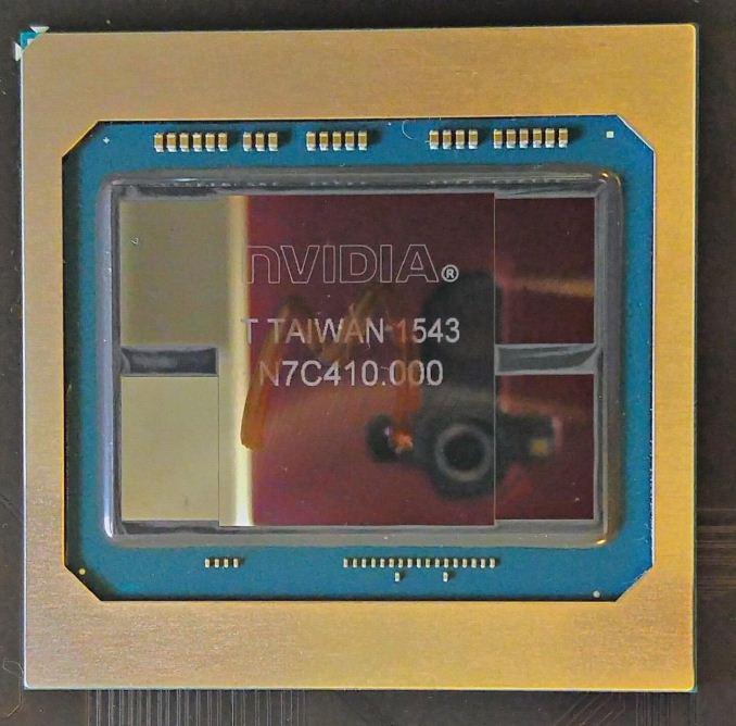
Over at the Hot Chips symposium Nvidia has been sharing a thing or two with media. Quite interesting is a new photo series of the GP100. Now do not confuse GP100 with the GP102 that is housed in the Nvidia Titan X (Pascal).

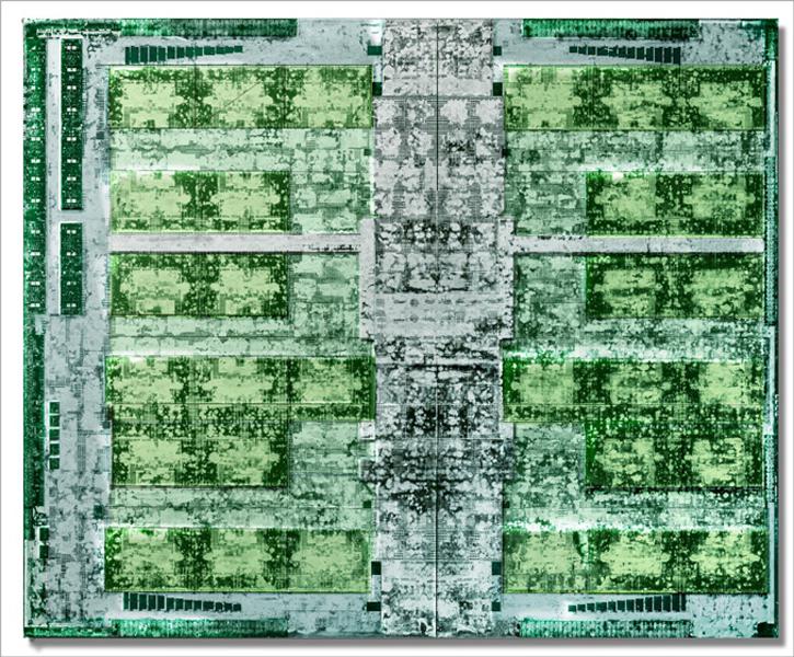
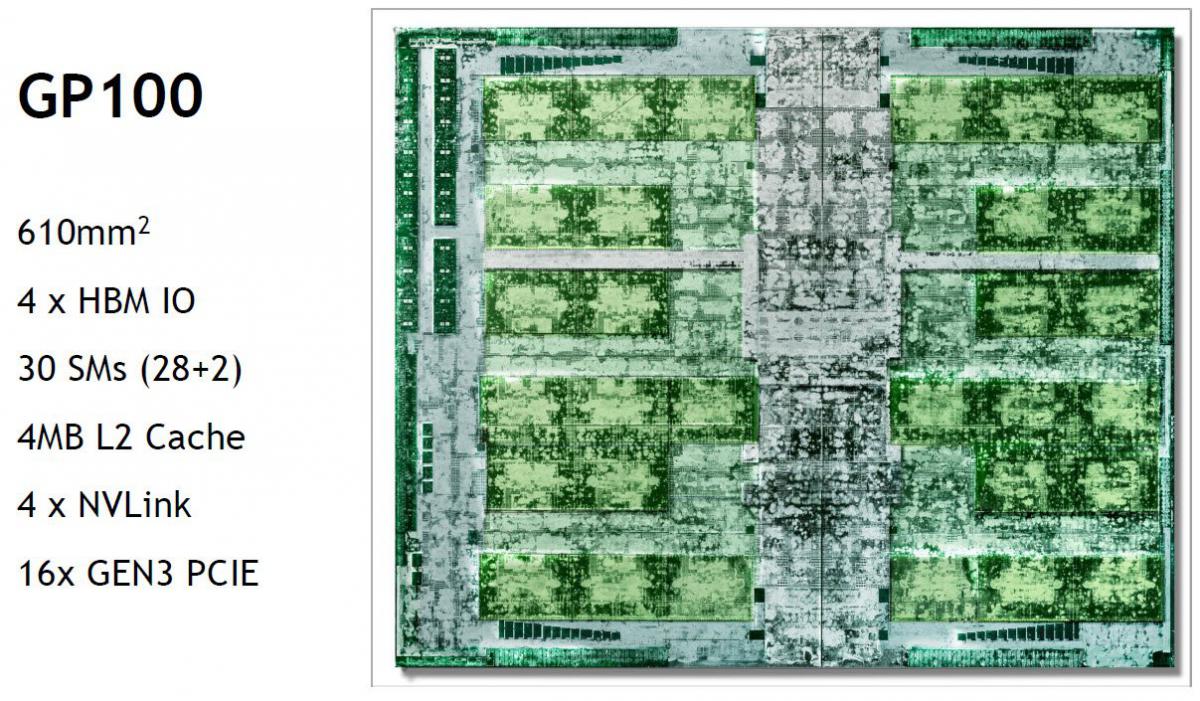
The GP100 is the GPU that houses HBM2 is referred to as BIG Pascal. Ryan over at Anandtech posted an actual die shot of the graphics processor, and man that thing is just HUGE as it is 610mm2. Big Pascal made on TSMC's 16 nanometer silicon fab process. 

Ya'll ready? here it is:

 
GP100 in particular comes with stacked HBM2 (16GB in four stacks). The Pascal based GPU driving the unit holds 15 Billion transistors which is roughly double that of the current biggest Maxwell chip. Gp100 is huge at 610mm^2. The prognosis performance (according to Nvidia) is 5.3TFLOPS using 64-bit floating-point numbers and is rated at 10.6TFLOPS using 32-bit and 21.2TFLOPS using 16-bit. P100 has 4MB of L2 cache and 14MB of shared memory for just the register file. The following table provides a high-level comparison of Tesla P100 specifications compared to previous-generation Tesla GPU accelerators, I added the GP100 as a fully enabled product:

Tesla Products Tesla K40 Tesla M40 Tesla P100 GP100
GPU GK110 (Kepler) GM200 (Maxwell) GP100 (Pascal) GP100 (Pascal)
SMs 15 24 56 60
TPCs 15 24 28 30
FP32 CUDA Cores / SM 192 128 64 64
FP32 CUDA Cores / GPU 2880 3072 3584 3840
FP64 CUDA Cores / SM 64 4 32 32
FP64 CUDA Cores / GPU 960 96 1792 1920
Base Clock 745 MHz 948 MHz 1328 MHz ~1328 MHz
GPU Boost Clock 810/875 MHz  1114 MHz 1480 MHz ~1480 MHz
Texture Units 240 192 224 240
Memory Interface 384-bit GDDR5 384-bit GDDR5 4096-bit HBM2 4096-bit HBM2
Memory Size Up to 12 GB Up to 24 GB 16 GB 16 GB
L2 Cache Size 1536 KB 3072 KB 4096 KB 4096 KB
Register File Size / SM 256 KB 256 KB 256 KB 256 KB
Register File Size / GPU 3840 KB 6144 KB 14336 KB 14336 KB
TDP 235 Watts 250 Watts 300 Watts ~300 Watts
Transistors 7.1 billion 8 billion 15.3 billion 15.3 billion
GPU Die Size 551 mm² 601 mm² 610 mm² 610 mm²
Manufacturing Process 28-nm 28-nm 16-nm 16-nm

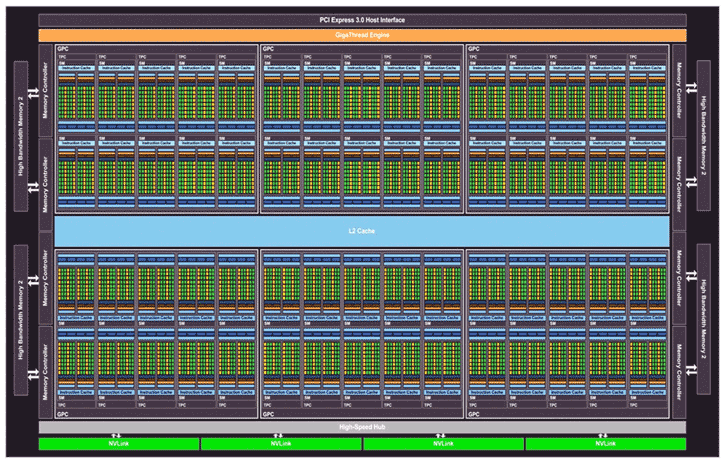
As the block diagram now shows, the GP100 features six graphics processing clusters (GPCs). Just look at the diagram and count that each GPC holds 10 streaming multiprocessors (SMs) and then each SM has 64 CUDA cores and four texture units. Do the math and you'll reach 640 shader processors per GPC and 3840 shader cores with 240 texture units in total. 6 (GPC) x (10x64) = 3840 Shader processor units in total. Some additional photos can be spotted below including an actual photo of the GP100 silicon. Click the thumbnails to enlarge.


Nvidia Pascal GP100 Die Shot Photo Nvidia Pascal GP100 Die Shot Photo Nvidia Pascal GP100 Die Shot Photo


« Obduction is now available · Nvidia Pascal GP100 Die Shot Photo · PCI Express 4.0 Will Deliver 75 Watt over PCIe not 300W »

Related Stories

Nvidia Pascal GP104-400 GPU photo surfaces and shows GDDR5X Memory - 04/25/2016 08:45 AM
Yet another PCB photo appeared with on it, a GPU seated. This time it is the  GP104-400-A1 GPU which which would be the 3rd Pascal GPU surfacing, and kind of seems to cinfirm a 980 Ti succesor, the ...

NVIDIA partners halt GeForce GTX 970, 980, 980Ti production and GPU Pascal codenames surface - 04/13/2016 08:25 AM
In anticipation of upcoming Pascal products in the coming month or two, at least that's what hwbattle is reporting this morning. As we get closer to the actual launch more and more tiny little detai...

Nvidia Pascal Consumer card announced during Computex - 04/11/2016 01:48 PM
But they will launch later ... Nvidia is to announce its consumer grade Pascal graphics cards at Computex 2016 from May 31-June 4, graphics card manufacturers include Asus, Gigabyte and MSI. They wou...

NVIDIA Pascal GP104 Die Photo - 04/11/2016 09:39 AM
Last week Nvidia announced the Tesla P100 data-center GPU and if you looked closely at the photo's you could already clearly see that big Pascal 15B transistor GPU being used. A new photo this time...

Judge rules that Samsung and Qualcomm do not violate Nvidia patents - 10/12/2015 08:10 AM
According to a judge ruling from the International Trade Commission, Samsung and Qualcomm do not violate Nvidia patents. Nvidia released this news themselves on their blog. Nvidia will appeal this r...


3 pages 1 2 3


rl66
Senior Member


Posts: 2740
Joined: 2007-05-31

#5326108 Posted on: 08/25/2016 09:26 AM
There is 2 tesla version of pascal, one cut down and one full, the info are on the dedicated website (the cut down have less hbm2 memory too btw).

TheDeeGee
Senior Member


Posts: 6968
Joined: 2010-08-28

#5326110 Posted on: 08/25/2016 09:27 AM
Dat TDP tho, the same as my entire system :P

icedman
Senior Member


Posts: 1071
Joined: 2013-02-22

#5326117 Posted on: 08/25/2016 09:51 AM
I'm confused is this supposed to replace the current titan, is it the 1080ti, or both and anyone that already bought a titan has been screwed just like very first titan lol

Xionor
Member


Posts: 33
Joined: 2016-03-24

#5326133 Posted on: 08/25/2016 10:45 AM
I'm confused is this supposed to replace the current titan, is it the 1080ti, or both and anyone that already bought a titan has been screwed just like very first titan lol


The only people that actually need a Titan, and have a Titan, have more than enough money for another Titan.

DeskStar
Senior Member


Posts: 1117
Joined: 2011-01-11

#5326163 Posted on: 08/25/2016 12:14 PM
The only people that actually need a Titan, and have a Titan, have more than enough money for another Titan.


Here......HERE..!!!!

3 pages 1 2 3


Post New Comment
Click here to post a comment for this news story on the message forum.


Guru3D.com © 2021