Micron Starts Sampling GDDR5X Memory to Customers
Way ahead of schedule (the target was late Summer) Micron has started shipping GDDR5X Memory its customers, likely Nvidia first. Micron will offer the ICs in 8 Gb (1 GB) and 16 Gb (2 GB) densities which indeed is indicative for 8GB adn 16GB graphics cards. The upcoming GeForce GTX 1070 and 1080 (if they are named that) already have been indicated as 8GB products.
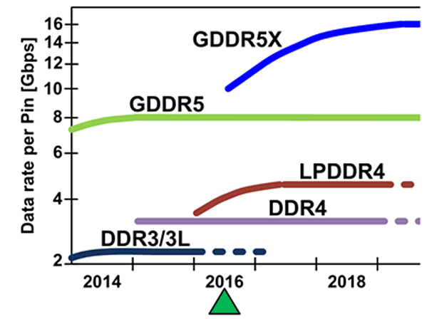
GDDR5X is your standard GDDR5 memory however, opposed to delivering 32 byte/access to the memory cells, this is doubled up towards 64 byte/access. And that in theory could double up graphics card memory bandwidth. Early indications according to the presentation show numbers with the memory capable of doing up-to 10 to 12 Gbps, and in the future 16 Gbps. So your high-end graphics cardsthese days hover at say 400 GB/s. With GDDR5X that could increase to 800~1000 GB/sec and thus these are very significant improvements, actually they are competitive enough with HBM.
The big advantage of 64 byte/access GDDR5X is that it doesn't need hefty design changes other it would need compatible memory controllers, so this might be a very cost efficient methodology until HBM has matured and will be a more affordable solution.
AMD and NVIDIA are working on GDDR5X support.
Told ya ;)
Senior Member
Posts: 1616
Joined: 2012-10-07
It doesn't matter though does it? Just need to make sure there's enough bandwidth available for the core - does it really matter if they do that through better VRAM or through memory bus widening?
Senior Member
Posts: 11809
Joined: 2012-07-20
GDDR5 has 170 pins per package, GDDR5X has 190 pins per package. Their prognosis for early chips is 25% higher throughput per pin.
Signaling pin count went up from 67 to 68 which does not increase complexity of PCB.
Means one chip should deliver 1.25 * 190/170 = 1.397 ~ 40% higher transfer rate than GDDR5 standard package.
Or does that mean 1.25 * 68/67 = 1.269 ~ 27% higher transfer rate than GDDR5 standard package?
Number of pins goes apparently up by ~12%. Chip is accessible in x32 and x16 mode (faster and slower). But signaling pin count stays practically same, so PCB complexity stays same per memory chip.
x16 mode is to allow communication through lower amount of traces (lower speed), but to allow another set of traces to connect another chip ("doubling" capacity per traces used).
- In reality one GDDR5X is connected in standard way and another is connected behind it (easily on other side of PCB).
I can see potential for next GTX970. While memory controller may be 384bit, 2 chips will share traces for higher capacity. I'll keep an eye on memory layout from now on when I check GDDR5X graphics cards.
- this sharing is done in following way:
- > GDDR5X uses 4 data and 4 error correction channels, has command and address bus
- > in x16 mode 1st memory chip gets 2 out of 4 data and 2 out of 4 error correction channels. 2nd chip gets another 2 of each. 1st chip gets command and address bus and relays required information to 2nd chip if appropriate (extra latency?).
Edit: Actually little correction for underlined text:
It seems that command and address bus is directly shared, so there is another logic behind which tells chips if command is for them (maybe both read required address and check if it is in their scope). (still extra latency)
Member
Posts: 37
Joined: 2016-03-24
Well this suddenly makes the recent Geforce X80 leaks very plausible.
(Lurker for many years, first post ever.)
Senior Member
Posts: 1616
Joined: 2012-10-07
GDDR5 has 170 pins per package, GDDR5X has 190 pins per package. Their prognosis for early chips is 25% higher throughput per pin.
Signaling pin count went up from 67 to 68 which does not increase complexity of PCB.
Means one chip should deliver 1.25 * 190/170 = 1.397 ~ 40% higher transfer rate than GDDR5 standard package.
Or does that mean 1.25 * 68/67 = 1.269 ~ 27% higher transfer rate than GDDR5 standard package?
Number of pins goes apparently up by ~12%. Chip is accessible in x32 and x16 mode (faster and slower). But signaling pin count stays practically same, so PCB complexity stays same per memory chip.
x16 mode is to allow communication through lower amount of traces (lower speed), but to allow another set of traces to connect another chip ("doubling" capacity per traces used).
- In reality one GDDR5X is connected in standard way and another is connected behind it (easily on other side of PCB).
I can see potential for next GTX970. While memory controller may be 384bit, 2 chips will share traces for higher capacity. I'll keep an eye on memory layout from now on when I check GDDR5X graphics cards.
- this sharing is done in following way:
- > GDDR5X uses 4 data and 4 error correction channels, has command and address bus
- > in x16 mode 1st memory chip gets 2 out of 4 data and 2 out of 4 error correction channels. 2nd chip gets another 2 of each. 1st chip gets command and address bus and relays required information to 2nd chip if appropriate (extra latency?).
Edit: Actually little correction for underlined text:
It seems that command and address bus is directly shared, so there is another logic behind which tells chips if command is for them (maybe both read required address and check if it is in their scope). (still extra latency)
Well I don't understand all that, but I have heard that GDDR5x is supposed to be offering twice the bandwidth of current GDDR5 (in addition to that same 'fact' being mentioned in this article) - through greater efficiencies mainly, but also through higher clock speeds.
Senior Member
Posts: 2952
Joined: 2013-03-10
Can't the manufacturers just use it for their profit by further cutting the memory bus width since less can give the same result if its faster? They seem to like doing that of late.