JEDEC announced the publication of JESD232 Graphics Double Data Rate (GDDR5X) SGRAM. Available for free download from the JEDEC website, the new memory standard is designed to satisfy the increasing need for more memory bandwidth in graphics, gaming, compute, and networking applications.
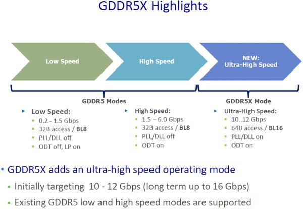
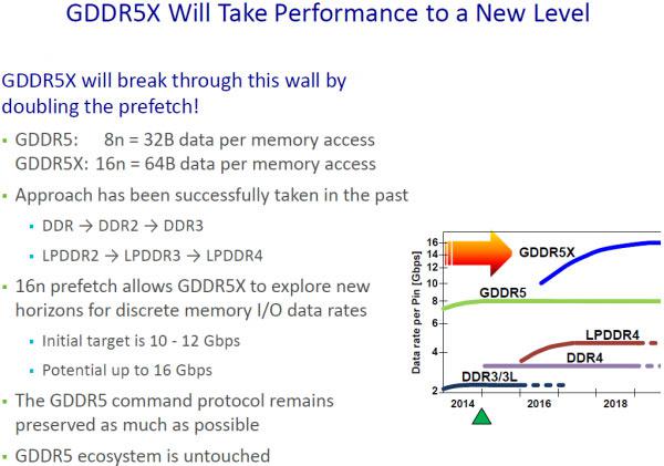
GDDR5X is your standard GDDR5 memory however, opposed to delivering 32 byte/access to the memory cells, this is doubled up towards 64 byte/access. And that in theory could double up graphics card memory bandwith. Early indications according to the presentation show numbers with the memory capable of doing up-to 10 to 12 Gbps, and in the future 16 Gbps. So your high-end graphics cardsthese days hover at say 400 GB/s. With GDDR5X that could increase to 800~1000 GB/sec and thus these are very significant improvements, actually they are competitive enough with HBM.
Jedec:
Derived from the widely adopted GDDR5 SGRAM JEDEC standard, GDDR5X specifies key elements related to the design and operability of memory chips for applications requiring very high memory bandwidth. With the intent to address the needs of high-performance applications demanding ever higher data rates, GDDR5X is targeting data rates of 10 to 14 Gb/s, a 2X increase over GDDR5. In order to allow a smooth transition from GDDR5, GDDR5X utilizes the same, proven pseudo open drain (POD) signaling as GDDR5.
“GDDR5X represents a significant leap forward for high end GPU design,” said Mian Quddus, JEDEC Board of Directors Chairman. “Its performance improvements over the prior standard will help enable the next generation of graphics and other high-performance applications.”
About JEDEC
JEDEC is the global leader in the development of standards for the microelectronics industry. Thousands of volunteers representing nearly 300 member companies work together in 50 JEDEC committees to meet the needs of every segment of the industry, manufacturers and consumers alike. The publications and standards generated by JEDEC committees are accepted throughout the world. All JEDEC standards are available for free download from the JEDEC website.
JEDEC Announces Publication of GDDR5X Graphics Memory Standard