Guru3D.com
  • HOME
  • NEWS
    • Channels
    • Archive
  • DOWNLOADS
    • New Downloads
    • Categories
    • Archive
  • GAME REVIEWS
  • ARTICLES
    • Rig of the Month
    • Join ROTM
    • PC Buyers Guide
    • Guru3D VGA Charts
    • Editorials
    • Dated content
  • HARDWARE REVIEWS
    • Videocards
    • Processors
    • Audio
    • Motherboards
    • Memory and Flash
    • SSD Storage
    • Chassis
    • Media Players
    • Power Supply
    • Laptop and Mobile
    • Smartphone
    • Networking
    • Keyboard Mouse
    • Cooling
    • Search articles
    • Knowledgebase
    • More Categories
  • FORUMS
  • NEWSLETTER
  • CONTACT

New Reviews
Fractal Design Focus 2 chassis review
Scythe Mugen 5 Rev.C CPU Cooler review
be quiet Pure Loop 2 FX 280mm LCS review
HP FX900 1 TB NVMe Review
Scythe FUMA2 Rev.B CPU Cooler review
SK Hynix Platinum P41 2TB M.2 NVMe SSD Review
Corsair K70 RGB PRO Mini Wireless review
MSI MPG A1000G - 1000W PSU Review
Goodram IRDM PRO M.2 SSD 2 TB NVMe SSD Review
Samsung T7 Shield Portable 1TB USB SSD review

New Downloads
Corsair Utility Engine Download (iCUE) Download v4.27.168
Download Intel network driver package 27.6
AMD Radeon Software Adrenalin 22.8.1 driver download
Prime95 download version 30.8 build 16
Memtest86 9.5 download
Intel ARC graphics Driver Download Version: 30.0.101.1743
GeForce 516.94 WHQL driver download
Display Driver Uninstaller Download version 18.0.5.4
FurMark Download v1.31
Intel HD graphics Driver Download Version: 31.0.101.3222


New Forum Topics
Intel Core i9-13900K could get extreme performance mode at 350 Watt TDP Photo of an Actual AMD Ryzen 7 7700X FSR Thread AUKEY USB Type-C cable has digital display showing real-time power up to 100W Does MSI Afterburner "bypass" the fan stop feature? 7-Zip decompression speed test, the Intel Core i9-13900K is 60% faster than the i9-12900K. [3rd-Party Driver] Amernime Zone Radeon Release Nemesis 22.6.1 WHQL DriverPack (22.7.1 pending ...) Display Driver Uninstaller Thread ASUS AMD X670E Motherboards Start listing at $670 AMD Will Announce New Ryzen Processors during August 29 Livestream Event


Guru3D.com » News » Japan with USA want to produce cutting-edge 2-nm chips as soon as 2025

Japan with USA want to produce cutting-edge 2-nm chips as soon as 2025

by Hilbert Hagedoorn on: 06/16/2022 08:08 AM | source: nikkei.com | 14 comment(s)
Japan with USA want to produce cutting-edge 2-nm chips as soon as 2025

Japan and the US have signed a bilateral chip technology partnership. This could end up as a joint venture between Japanese and US firms, or a wholly Japanese-owned setup. Semiconductors could be used for everything from quantum computers to smartphones.

TOKYO -- Japan will work with the U.S. to launch a domestic manufacturing base for 2-nanometer semiconductors as early as fiscal 2025, Nikkei has learned, joining the race for commercializing the next-generation chip technology.

Tokyo and Washington will provide support under a bilateral chip technology partnership. Private companies from the two countries will pursue research on design and mass production.

Taiwan Semiconductor Manufacturing Co. is ahead in developing mass production technology for 2-nm chips. Japan seeks to secure a stable supply of semiconductors by realizing domestic production of the next-generation chips.

Japanese and U.S. businesses could jointly establish a new company, or Japanese corporations could set up a new manufacturing hub. Japan's Ministry of Economy, Trade and Industry will partially subsidize the cost of research and development as well as capital expenditures.

Joint research will start this summer at the earliest, and a research and mass production center will be formed between fiscal 2025 and fiscal 2027.

TSMC, the world's largest contract chip manufacturer, is building a chip fab in Japan's Kumamoto Prefecture, but the plant will only produce less-advanced semiconductors scaled from 10nm to the 20nm range.

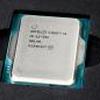
Smaller semiconductors lead to miniaturization and improved performance of devices. The 2-nm chips will be used in products such as quantum computers, data centers and cutting-edge smartphones. Those chips also reduce power consumption, shrinking carbon footprints.

The size can determine the performance of military hardware as well, including fighter jets and missiles. In that light, 2-nm chips are directly linked to national security.

In early May, Japan and the U.S. signed basic principles on semiconductor cooperation. The two sides will discuss the finer points of the cooperative framework during an upcoming "two-plus-two" meeting of cabinet economic officials.

Prime Minister Fumio Kishida's "new capitalism" agenda, approved by the cabinet last week, outlines the formation of a design and manufacturing base this decade through a bilateral public-private collaboration with the U.S.

IBM, which is strong in 2-nm R&D, developed a prototype last year. Fellow U.S. company Intel also is proceeding with R&D on the 2-nm process.

In Japan, a research lab in Tsukuba city run by the National Institute of Advanced Industrial Science and Technology is hosting a collaboration to develop manufacturing technology for advanced semiconductor lines, including those for 2-nm processes. Chipmaking equipment makers like Tokyo Electron and Canon are taking part in the collective, along with IBM, Intel and TSMC.

Japan is home to strong chip materials makers such as Shin-Etsu Chemical and Sumco, while the U.S. has the chipmaking equipment giant Applied Materials. This cooperation between chipmakers and key suppliers is intended to put mass production tech for 2-nm chips within reach.

TSMC sits at the forefront of mass production of next-generation chips. The company is expected to break ground this year on a 2-nm fabrication facility and expects to begin large-scale manufacturing of 3-nm chips later this year.


« AGON by AOC Launches AGON PRO AG344UXM with 170Hz MiniLED Panel · Japan with USA want to produce cutting-edge 2-nm chips as soon as 2025 · TerraMaster T6-423 Professional NAS and TOS 5 Operating System »

3 pages 1 2 3


Valken
Senior Member


Posts: 2203
Joined: 2011-01-05

#6025781 Posted on: 06/16/2022 02:16 PM
Godzilla, quakes, tsunamis, nuclear meltdown, yup, makes sense...

Brasky
Senior Member


Posts: 2403
Joined: 2011-05-19

#6025785 Posted on: 06/16/2022 02:21 PM
That's good news for everyone, we (the world) need another few powerhouse chip production locations for when China invades the sovereign country of Taiwan.

JamesSneed
Senior Member


Posts: 1497
Joined: 2017-02-14

#6025794 Posted on: 06/16/2022 02:53 PM
That's good news for everyone, we (the world) need another few powerhouse chip production locations for when China invades the sovereign country of Taiwan.


I keep watching the news for this and man it keeps escalating day by day. Verry worrysome.

schmidtbag
Senior Member


Posts: 6689
Joined: 2012-11-10

#6025806 Posted on: 06/16/2022 03:29 PM
The article seems to imply there may be a new company - why not just dump the money into GloFo? Might be cheaper, and it would be a little sad for them to be pushed even further behind than they are now.

tunejunky
Senior Member


Posts: 2546
Joined: 2017-08-18

#6025825 Posted on: 06/16/2022 04:45 PM
The article seems to imply there may be a new company - why not just dump the money into GloFo? Might be cheaper, and it would be a little sad for them to be pushed even further behind than they are now.


despite the headline the true purpose is to ensure a US/Japanese source for advanced Lithography.

when every major competitor to ASML is American or Japanese (Applied Materials, KLA, Nikon, Canon) this begins to make sense.

after all there's no 2nm w/o EUV and this consortium can leverage all existing in-house R&D and keep clear of patents (otherwise they would announce licensing).
there is no fab without lithography and Intel has guaranteed ASML's future (but keeping single sourcing worries alive) to the tune of billions of dollars

3 pages 1 2 3


Post New Comment
Click here to post a comment for this news story on the message forum.


Guru3D.com © 2022