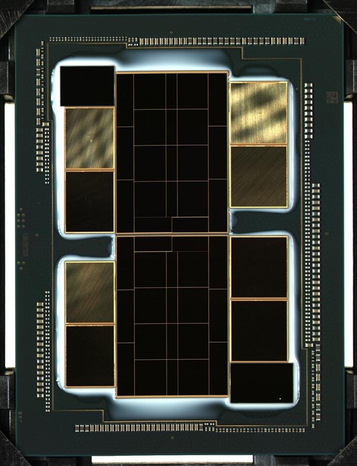
On Twitter Intel is showing a Xe HPC Multi-Chip Module photo (Ponte Vecchio), the tweet was made by Ex AMD's Raja Koduri. This is the first picture showing the chip that way as the heat spreader has been taken off.
The graphics processor is a multi-chip module and shows two very big main dies (7 nm) likely fabbed at TSMC. And no this is not a gamers processor, instead, it'll be targeted at datacenter centric environments. The package seems to be almost twice the size of what Nvidia's A100 top model for servers utilize.
You are looking at Frankenstein in a silicon form as seven advanced technologies into a single package have been applied, combined with four different production processes of the chips. What's interesting to see is that surrounding the two dies, you can see different sized memory chips. The square ones are HBM2/HBM3, the smaller ones we're not sure of. It could be GDDR DRAM functioning as some sort of cache, or even 3D XPoint, NAND flash in Intel's Foveros packaging. Anyway, an impressive setup none-the-less, feast away, here it is:
Intel Shows Xe HPC Multi-Chip Module Die