Intel delivered updates at its Technology and Manufacturing Day held in Beijing, China, on Sept. 19. Disclosures included power and performance updates for Intel’s 10 nm process, high-level plans for Intel’s first 10 nm FPGA, and an announcement that the company is shipping the industry’s first commercially available 64-layer 3D NAND for data center applications.
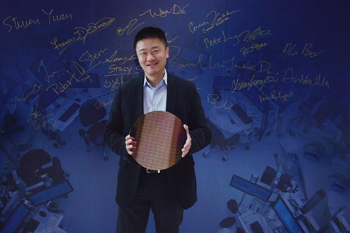
Demonstrating Intel’s technology lead, Intel Senior Fellow Mark Bohr presented specification updates showing Intel’s 10 nm is a full generation ahead of other “10 nm” technologies in terms of both transistor density and transistor performance. Intel’s 10 nm technology has the world’s tightest transistor and metal pitches, created with hyper scaling, for the highest density in the industry. Hyper scaling is a term used by Intel to describe the 2.7x logic transistor density improvement attained on the company’s 14 nm and 10 nm processes. And, for the first time, Intel’s “Cannon Lake” 10 nm wafer was on public display.
Bohr also provided power and performance updates for Intel’s 22FFL, a compelling lower-power FinFET technology for mobile applications first introduced at Intel’s Technology and Manufacturing Day in March in San Francisco. The updates included best-in-class CPU performance of more than 2 Ghz with ultra-low power of more than 100x lower leakage. In addition, a 22FFL wafer was on public display for the first time.
Intel unveiled high-level plans for its coming generation of FPGAs using the 10 nm process technology and foundry platform. Introduced under the code name “Falcon Mesa,” the FPGA will offer new levels of performance to support the growing bandwidth demands of data center, enterprise and networking environments. For more, read the Falcon Mesa fact sheet.
During the Intel Developer Forum in San Francisco in August 2016, Intel Custom Foundry announced an agreement with ARM* to accelerate the development and implementation of ARM SoCs on Intel’s 10 nm process. The results of this collaboration were highlighted with the display of a 10 nm test chip wafer containing ARM Cortex-A75 CPU cores implemented with industry standard design flows enabling performance in excess of 3 GHz.
Intel also announced that it is shipping of the industry’s first 64-layer, triple level cell (TLC), 3D NAND SSD (solid state drive) for data center applications. Designed to help customers significantly improve storage efficiency, the product has been shipping to select top-tier cloud service providers since early August. Intel’s three decades of developing expertise in memory has resulted in an optimized 3D NAND floating gate architecture and manufacturing process. This process leadership has enabled Intel to quickly expand its 64-layer TLC SSD portfolio from the client product, introduced in June, to now include SSDs for use in data centers. The product will be made more broadly available by the end of this year.
Intel Showcases 10nm Updates and 64-Layer NAND For Enterprise