Intel Likely Starts 10nm Volume Production in the second half of 2018
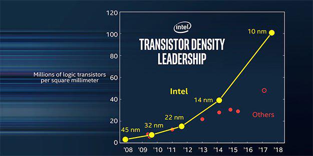
Intel is pushing hard with the production of 10nm processors, the chip yield is currently low, Intel delivers only a few CPUs to partners. Ice Lake is expected to appear in 2019.
The 10-nm series production is scheduled to start at Intel in the second half of 2018, which has announced CEO Brian Krzanich in discussing the results of the fourth quarter of 2017 mentions Golem. According to Krzanich, in the coming months, the chip yield (yield) will be increased dramatically for proper mass production, the manufacturer so far has sent only limited samples of Cannon Lake U to close partners.
Apparently, the plan is to switch from 10 nm to 10+ nm as quickly as possible, a slightly improved version of the fabrication node. Ice Lake is to be created with this production technology. Intel intends to use these processors in all segments from the tablet to up-to supercomputer.
For Ultrabooks, Intel is planning a follow-up to Whiskey Lake for Kaby Lake Refresh , another 15-watt quad-core. In addition to a 4 + 2 design with four cores and GT2 graphics unit is also one with 4 + 3 planned, but then called Coffee Lake U. This design uses a GT3, the more shader cores and also EDRAM as a fast On -Package memory uses. Whiskey Lake U and Coffee Lake U are apparently manufactured at 14++ nm.
For a higher class of performance, the Coffee Lake H are planned, which are Hexacore chips with 45 watts of thermal loss. They follow Kaby Lake H with four cores and are said to clock very high at up to 4.8 GHz . Top model will probably be the Core i9-8950HK with open multiplier for notebook overclockers. Thus far Intel uses the Core i9 designation only for desktop chips like the Core i9-7980XE with 18 CPU cores.
Intel likely to figure a way to keep LGA design for CPUs - 12/22/2012 09:58 AM
Commenting on Intel's reported plans of abandoning CPU socket designs and changing to directly soldered CPUs after two years, Asustek Computer vice president and general manager of motherboard/deskto...
Intel licenses ZiiLabs GPU technology - 11/21/2012 10:13 AM
If that sounds familiar, it's because it is. Intel has entered with Creative Technology to acquire GPU technologies and engineering resources from ZiiLabs, a wholly-owned UK-based subsidiary of Crea...
Intel Light Peak arrives in 2012 - 09/17/2010 10:57 AM
Intel demonstrated 10Gbps Light Peak at the IDF in San Francisco, the company said chips for the optical interconnect will be available in 2011 and the first computers with Light Peak could hit the ma...
Intel Light Peak doubles USB 3.0 speed - 04/16/2010 05:20 AM
There's probably a very good reason why Intel is trying to stall chipset support for USB 3.0, they'd like it much more if they could control the market with their own patents and licenses. But that do...
Intel likely to delay mainstream Core i7 to August - 01/17/2009 01:18 PM
Intel is likely to
Member
Posts: 80
Joined: 2009-10-01
Because transistors are not cubes. They have odd shapes and are susceptible to interference or electron tunneling if placed too close to one another. The drop is measured size vs. die area depends on which axis were shrunk and by how much. Their "size" is also measured differently by different companies. Intel's 14nm process is smaller than global foundries 14nm (which would be about 18nm if they were measured the way Intel measures). To get a better picture of the possible density we need to know the exact size along all three axis as well as the required void space between components to know how much area they use and how closely they can be packed. At the moment those details aren't available yet for the 10nm process, just the density.
Senior Member
Posts: 1458
Joined: 2017-02-14
Also recall when Intel moved to using FinFets back when they were at 22nm ie "transistors in the 3d dimension" they called it. People gloss over this all the time but now chips are 3d the nanometers taken from the smallest feature the lithography can make really doesn't mean much anymore. It meant a lot more back when chips were "2d" since it directly contributed to the gate length which had a fairly predictable shrink but it was mostly marketing then too. So the little fins that stick up like a microscopic sharks fin contribute a lot to density as well. Instead of just measuring width you now have to account for the length and the pitch or what angle the pieces lean over on the 3d pieces. I tried to keep this rather high level on purpose. The short of it is lithography feature size doesn't translate to densities anymore since chips are now in 3d.
Senior Member
Posts: 4385
Joined: 2004-12-13
Great explanation guys, thanks for helping us better understand what is going on!
Senior Member
Posts: 321
Joined: 2007-01-19
That graph is strange... how does moving from 14nm to 10nn more than double the transistor density(40mio/mm² @ 14nm -> 100mio/mm² @ 10nm = -28% size, 2.5x density)? Especially if the previous larger shrinks only allowed for a smaller improvement (18mio/mm² @ 22nm -> 40mio/mm² @ 14nm = -36% size, 2.22x density)