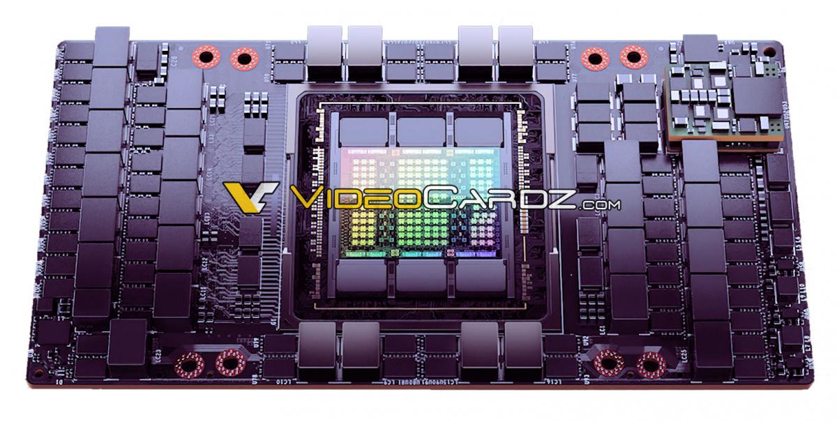
NVIDIA H100 Hopper computing processor replaces the two-year-old Ampere"A100 computer processor, is shown in this photograph for the first time. The proc will get 140 Billion transistors, compared to 54 Billion for the GA100.
Hopper compute architecture expands on the capabilities of the "Ampere" compute architecture, including the most powerful AI deep-learning compute gear, FP64 math capacity, and a variety of other features. According to the company, the "GH100" processor, which is constructed on the TSMC N5 (5 nm) node, has more than doubled the transistor count of the A100 processor, which is expected to reach roughly 140 billion transistors. GH100 is one of the first NVIDIA chips to include two different types of GPCs, making it one of the first of its kind. The graphics-related SMs of NVIDIA are housed in one of the six GPCs, while the compute-related SMs are housed in the other five. When it comes to graphics, the system managers will contain RT cores and other raster-related components, while the system managers for computation will comprise special-purpose tensor cores and FP64 SIMD units.
Including the graphics SM, the silicon has a total of 144 SMs) HBM3 is the interface for memory, which has a capacity of 6144 bits. The H100 is expected to be announced by NVIDIA later today, NVIDIA CEO Jensen Huang is expected to announce it during a special GTC 2022 opening keynote.
Images of NVIDIA Hopper H100 GPU Compute Processor Surface