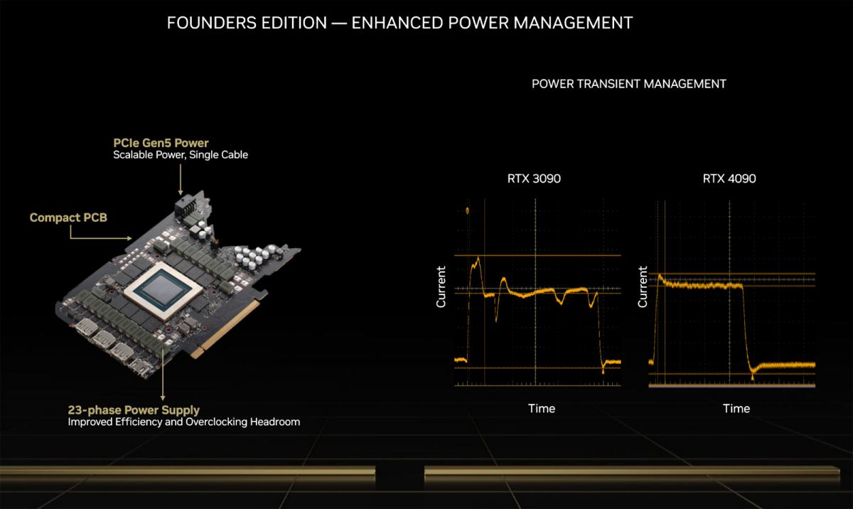
Nvidia unveiled the PCB design and other data for the GeForce RTX 4090 on Wednesday. To maximize GPU overclocking, the business upgraded the card's voltage regulating module (VRM) by adding a PID controller with a feedback loop.
The PCB includes a single 12+4-pin 12VHPWR extra PCIe Gen5 power connector capable of delivering up to 600W, while the default BIOS settings limit the GeForce RTX 4090 FE to 450W. The board's 20+3-phase VRM (20 phases for the GPU, 3 for memory) is an improvement over the 18+3-phase power circuitry found in the GeForce RTX 3090/3090 Ti FE. Nvidia also incorporated a PID controller with a feedback loop to reduce current spikes and drops. Nvidia claims that their new VRM decreases power management reaction time without offering specific figures. A clean power supply is required for stability under severe loads and overclocking. The green team employs 'power transient management' to increase the speed of its AD102 graphics processor to 3 GHz without overvolting or using harsh cooling.