
I've been doubting to post this news-item as the information is unsubstantiated and based on a very loose rumor from one website. But there currently is a rumor that GeForce GTX TITAN P would be announced at Gamescom. Personally I doubt it as it is way too soon, but hey I could be wrong here.
The news spreads based on a loose post on the source: VR World. Gamescom will be held in Cologne, Germany starting at the 17th of August. The rumor is that a card called GeForce GTX TITAN P (with the P for Pascal) will be announced, again I think it is too soon. That GP100 silicon would see light of day in two flavors, a 12 and 16 GB one. The 16 GB model would feature four HBM2 stacks over a 4096-bit memory bus; the 12 GB variant would feature three active HBM2 stacks and this would be based on a 3072-bit bus. Both similar to the Tesla P100-based PCIe super computer accelerators
The Pascal based GPU driving the unit holds 15 Billion transistors which is roughly double that of the current biggest Maxwell chip. Gp100 is huge at 600mm^2. The prognosis performance (according to Nvidia) is 5.3TFLOPS using 64-bit floating-point numbers and is rated at 10.6TFLOPS using 32-bit and 21.2TFLOPS using 16-bit. The P100 has 4MB of L2 cache and 14MB of shared memory for just the register file. The following table provides a high-level comparison of Tesla P100 specifications compared to previous-generation Tesla GPU accelerators, I added the GP100 as a fully enabled product in the following diagram to get an idea of what such a GPU would entail the GP100 might end up as GP102 (consumer chip) btw :
 |
||||
| Products | Tesla K40 | Tesla P100 | GP100 | GTX 1080 |
| GPU | GK110 (Kepler) | GP100 (Pascal) | GP100 (Pascal) | GP104 (Pascal) |
| SMs | 15 | 56 | 60 | 40 |
| TPCs | 15 | 28 | 30 | 20 |
| FP32 CUDA Cores / SM | 192 | 64 | 64 | 64 |
| FP32 CUDA Cores / GPU | 2880 | 3584 | 3840 | 2560 |
| Base Clock | 745 MHz | 1328 MHz | ~1328 MHz | 1607 MHz |
| GPU Boost Clock | 810/875 MHz | 1480 MHz | ~1480 MHz | 1733 MHz |
| Texture Units | 240 | 224 | 240 | 160 |
| Memory Interface | 384-bit GDDR5 | 4096-bit HBM2 | 4096-bit HBM2 | 256-bit |
| Memory Size | Up to 12 GB | 16 GB | 16 GB | 8 GB |
| L2 Cache Size | 1536 KB | 4096 KB | 4096 KB | 2048KB |
| Register File Size / SM | 256 KB | 256 KB | 256 KB | 256 KB |
| Register File Size / GPU | 3840 KB | 14336 KB | 14336 KB | 10240 KB |
| TDP | 235 Watts | 300 Watts | ~300 Watts | 180 Watts |
| Transistors | 7.1 billion | 15.3 billion | 15.3 billion | 7.2 Billion |
| Manufacturing Process | 28-nm | 16-nm | 16-nm | 16-nm |
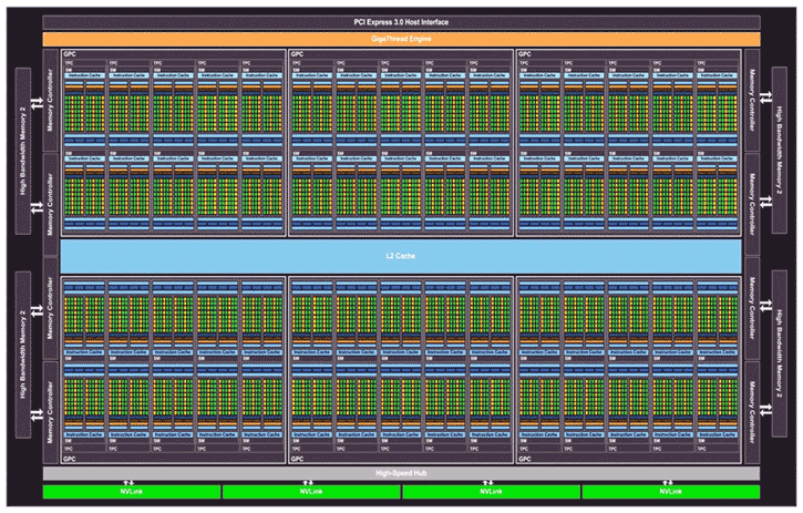
As the block diagram now shows, the GP100 features six graphics processing clusters (GPCs). Just look at the diagram and count along with me - each GPC holds 10 streaming multiprocessors (SMs) and then each SM has 64 CUDA cores and four texture units. Do the math and you'll reach 640 shader processors per GPC and 3840 shader cores with 240 texture units in total.
- 6 (GPC) x (10x64) = 3840 Shader processor units in total.
Meaning the GP100 used on the Tesla P100 is not fully enabled. Nvidia is known to out GPU that have disabled segments, it helps them selling different SKUs, the Tesla P100 holds a shader count of 3584 and thus has 56 SMs enabled (from the 60).
GP100’s SM incorporates 64 single-precision (FP32) CUDA Cores. In contrast, the Maxwell and Kepler SMs had 128 and 192 FP32 CUDA Cores, respectively. The GP100 SM is partitioned into two processing blocks, each having 32 single-precision CUDA Cores, an instruction buffer, a warp scheduler, and two dispatch units. While a GP100 SM has half the total number of CUDA Cores of a Maxwell SM, it maintains the same register file size and supports similar occupancy of warps and thread blocks.GP100’s SM has the same number of registers as Maxwell GM200 and Kepler GK110 SMs, but the entire GP100 GPU has far more SMs, and thus many more registers overall. This means threads across the GPU have access to more registers, and GP100 supports more threads, warps, and thread blocks in flight compared to prior GPU generations.
Since the graphics memory is on-die HBM2, the VRAM amount is fixed. That means that ALL GP100 products will get 16GB of memory or less. HBM2 will run a wide 4096-bit HBM2 (1024 bit per IC stack) memory interface running an effective bandwidth anywhere up-to a full 1 TB/s.
This is a big chip, very big at 600mm^2 hence it is interesting to see that 16nm can offer a lot in terms of clock frequency, The Tesla P100 is an enterprise part that ends up in servers, however this part already is clocked at 1328 MHz with Boost capabilities towards a frequency of 1480 MHz. Combined the TDP still remains to be under 300W.
GeForce GTX TITAN P might see August Announcement
