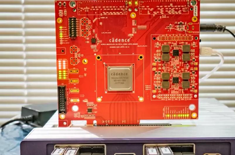
PCI Express 5.0, forget about it huh? PCI Express 6.0 is where we're headed already. Cadence developed one of the industry's first silicon-proven IP packages to help chip designers integrate and test PCIe 6.0 functionality.
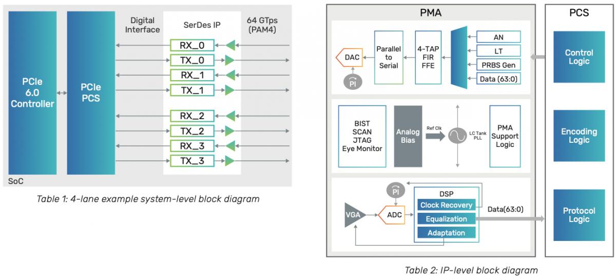
The IP is currently available and will allow early adopters to implement PCIe 6.0 in 2022-2023. It includes a controller and DSP-based PHY (physical interface). A multi-packet processing architecture allows up to 1024-bit wide data paths in x16 configuration, as well as all PCIe 6.0 capabilities, including up to 64 GT/s data transfer rate (both directions), PAM4 signaling, low-latency forward error correction (FEC), FLIT mode, and L0p power state. ASIC designers who need to support PCIe 6.0 as soon as possible might use the IP built for TSMC's N5 node. Cadence also offers a PCIe 6.0 test chip based on N5 that can evaluate signal integrity and performance at all data rates, reports toms hardware.
With a PAM4/NRZ dual-mode transmitter and a receiver that can survive extreme signal impairments and channel loss in excess of 35dB at 64GT/s, the device has sophisticated data recovery capabilities. Data transfers of up to 64 GT/s over relatively lengthy traces (DDR5 memory currently has a transfer rate of 4.8–7.0 GT/s) necessitate preserving signal integrity and enabling advanced data recovery procedures.
See this is the beauty of technology, it never stops evolving and developping.
Early Adopters Can Purchase PCIe 6.0 Chip Design Kits