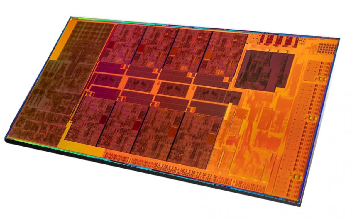
Intel yesterday 'somewhat' introduced Rocket Lake-S 14nm fabricated desktop processors. The processors are due for release somewhere in March. Alongside the presentation, a die shot was shared by Intel, and that one got dissected on social media creating an interesting picture of the processor die.
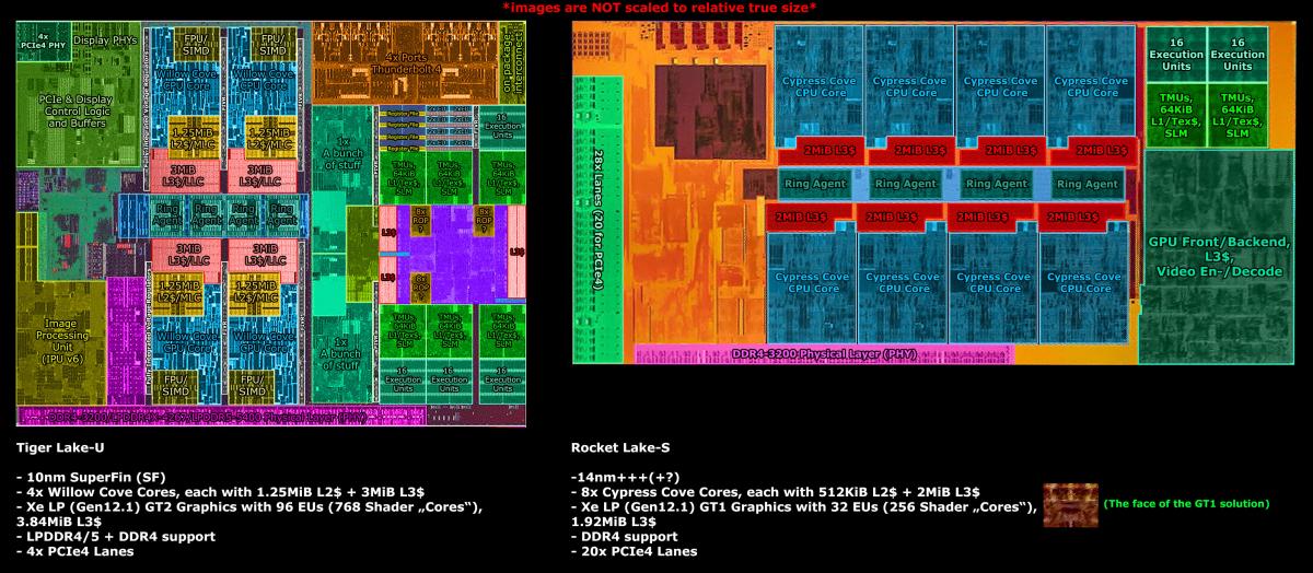
@Locuza_ on Twitter took the photo of the die and started dissecting the parts and blocks, obviously showing the eight Cypress Cove CPU cores and iGPU based on Xe. Cypress Cove cores have 512 KB of dedicated L2 cache. The shared L3 cache is 16 MB, spread across eight 2 MB slices. A big chunk of the silicon collateral goes to the Xe iGP ( Gen12 Xe-LP GT1 integrated graphics) with its 32 EUs (execution units) and thus 256 Shader processors. IO wise, there are 28 CPie gen 4.0 lanes, of which 20 can be used on the user end. Have a peek:
Breakdown Diagram of Intel Rocket-Lake S Die