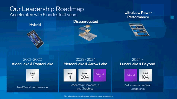
TSMC's new N2 node will be used by Apple and Intel, according to reports and sources in the financial world. N2 is TSMC's first manufacturing process to use the GAAFET (Gate-All-Around Field-Effect Transistor) design. By the end of 2025, it should be in wide use.
TSMC will be late to the GAAFET party. Samsung's 3GAE node will come out in 2023, and Intel's first Angstrom-era process, Intel 20A, will come out in 2024.
"We also see more clarity around TSMC's N2 expansion schedule in Fab 20 (Hsinchu)," Sze Ho Ng, an analyst with China Renaissance Securities, wrote in a note for clients. "Tool move-in is expected to start by end-2022, based on company plans, ahead of risk production in late 2024E with Intel (client PC Lunar Lake's graphic 'tiles', while the CPU 'tiles' are fabbed using Intel’s 18A) and Apple being the anchor customers for dedicated capacity support."
Intel's own slide that talks about the graphics tiles of Meteor Lake, Arrow Lake, and Lunar Lake processors clearly says that the latter's GPU will be made outside of the computer. This is because Intel's own technology is better than N3.
AMD, Broadcom, Nvidia, and MediaTek have all said that they will use different nodes from TSMC's N5 family (N5, N5P, N4, N4P, N4X). MediaTek has already formally announced its Dimensity 8000/8100 application processors and Dimensity 9000 SoC. Nvidia, on the other hand, will use a custom 4N fabrication process for its Hopper and presumably Ada Lovelace GPUs, which will be made in a different way. Also, AMD will make its Genoa and Raphael processors with a 5 nm process.
In a report from DigiTimes, all of these companies are in talks with TSMC about getting N3-capable capacity from the company in late 2020 or early 2024. In addition, these companies are also expected to start talking about N2-capable allocations next year. Apple and Intel, on the other hand, will be the first to use N2.
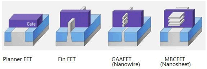
First, TSMC will use gate-all-around field-effect transistors (GAAFET) in its N2 technology. This is years after Samsung's 3GAE and more than a year after Intel's 20A technology, which both used this type of technology (2024). In terms of power, performance, and area/transistor density, the world's largest contract chip maker hasn't said what to expect from N2 over N3. However, because this will be a new node, it is reasonable to think that it will be better than its predecessors. The new process will still use the same extreme ultraviolet (EUV) lithography scanners that have a 0.33 numerical aperture. Intel's 18A, on the other hand, is set to use ASML's Twinscan EXE EUV scanners with High-NA (0.55NA).
Apple and Intel will be the first customers for TSMC's new 2 nm manufacturing node.