Alright, intriguing story and observation. Try to follow me. It seems that Radeon RX Vega 10 GPUs used on Radeon RX Vega 64 differ a little, I’ll step that up a notch, the seems to even be differing a little bit in height. And that might be relevant for the AIB cards.
Earlier on in our forums a user already asked if we had a different sample, he noticed that the GPU looks different compared to some other websites. After inspecting our review kit dummy sample and the one used on our graphics card sample I noticed it definitely differ. After further inspection I also noticed that the GPU that is used on our Vega 64 sample, differs from other reviewers. Now here's the thing, my Dutch colleagues over at Tweakers.net noticed something similar. It seems that AMD fabbing Vega at two different locations. And there is a significant enough physical difference:
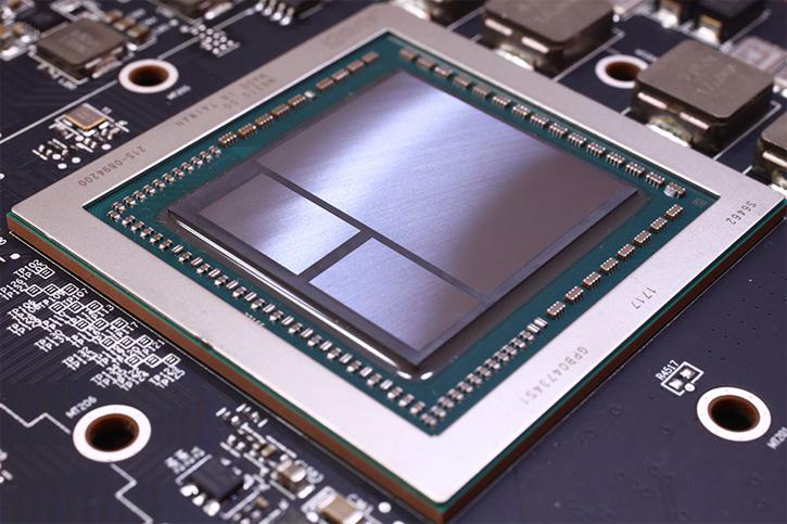
Have a look at the above photo, that’s one of the photos I made of the dummy (but real Vega10 GPU) GPU that AMD submitted as a bit of a fun teaser. See that black coating in-between the chips? Now look at the photo below.
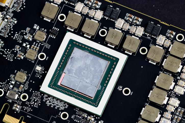
Compare the two, this photo I made from our Vega 64 graphics card sample, it’s just not the same is it? There should be a dark substrate in-between the HBM2 memory as you can clearly see on the upper photo, the 'dark stuff' is clearly missing on the second (pink area).
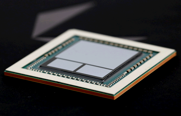
Now check out the upper photo, this one is courtesy from our colleagues at TPU, you can see that their Vega 64 sample is using the first model, totally different from my sample. And now finally, take a peek at the next one:
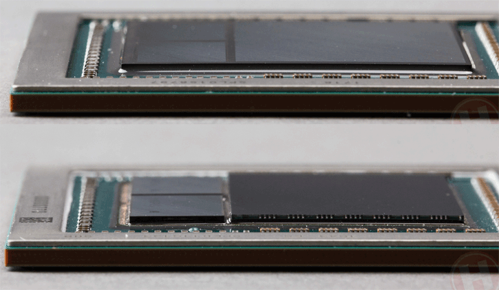
Now this photo is the very interesting, it is the dummy GPU from Dutch websites Tweakers and Hardware.info combined (photo courtesy goes out to them). Both websites share the same office and have the same boss, but both received a sample kit. By comparing the two GPUs directly towards each other you can see there is a bit of a height difference? It looks like the HBM2 is sitting a slight notch lower compared toward the GPU die right?
I have no idea what the tolerances are or that the angle of the photos trick the eyes a bit, but this is going to be interesting for the board partners as that difference might have an effect on cooling and in the end tweaking performance. The difference is so incredibly small that a bit of thermal compound likely would make this observation irrelevant. Also it simply does not make sense that HBM2 on part A is sitting higher or lower compared to part B, as in the end it's the same materials used.
But the fact remains, the GPU packages do differ.
Update: We've received word back from AMD, I'll just leave that here:
We have multiple manufacturing partners for Vega10 package assembly. To meet the high-volume production that we target with Vega10, we need access to most of the world capacity for 2.5D interposer technology. Each partner has unique processes, including one which has an epoxy fill to level the entire SOC surface. This specificity is inconsequential to the system solution and all Vega10 packages are form, fit and function equivalent. As there is no functional difference, any Vega10 package flavor can be binned into a Vega10 XL, XT or XTX.
AMD Radeon RX Vega 10 chips differ - physically and quite significantly (Updated)