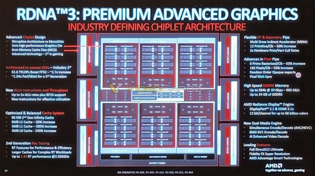
During last week's presentation, some had hopes for PCIe Gen 5.0 connectivity. However, the presentation and slides did not mention a thing about the version used. A newly leaked block diagram however confirmed this to be PCE Gen 4.0.
The alledged slide reveals the NAVI31" MCM, which has a core graphics compute die (GCD) chiplet made on the 5 nm EUV silicon fabrication process and is surrounded by six memory cache dies (MCDs) made on the 6 nm process. The GCD is linked to the system by way of a PCI-Express 4.0 x16 host interface. It has a new multimedia engine with dual-stream encoders and a new display engine called Radiance that works with DisplayPort 2.1 and HDMI 2.1a. Custom interconnects link it to the six MCDs.
Each MCD has a 16 MB Infinity Cache (L3 cache) and a 64-bit GDDR6 memory interface (two 32-bit GDDR6 paths). The 384-bit GDDR6 memory interface on the GPU is made up of six of these. The GCD has six Shader Engines, and each one has 16 compute units (or 8 pairs of compute units), for a total of 1,024 stream processors. AMD says that these stream processors are four times as fast as RDNA2. As you can see to the lower left block, it connects over PCIe gen 4.0.
AMD Navi 31 GPU Block Diagram Leaks, indeed PCIe gen 4.0