Fractal Design Meshify 2 Compact chassis review
Sabrent Rocket 4 PLUS 2TB NVMe SSD review
MSI Radeon RX 6900 XT GAMING X TRIO review
Guru3D Q1 Winter 20/21 PC Buyer Guide
AOC CU34G2X monitor review
Silicon Power UD70 PCIe 3.0 NVMe SSD review
Patriot Viper Steel RGB 3600 MHz (2x 16GB) review
ClockTuner 2.0 for Ryzen (CTR) Guide
Silicon Power US70 PCIe 4.0 NVMe review
Guru3D Rig of the Month - January 2021
AMD Moving to 12nm Vega and Ryzen in 2018
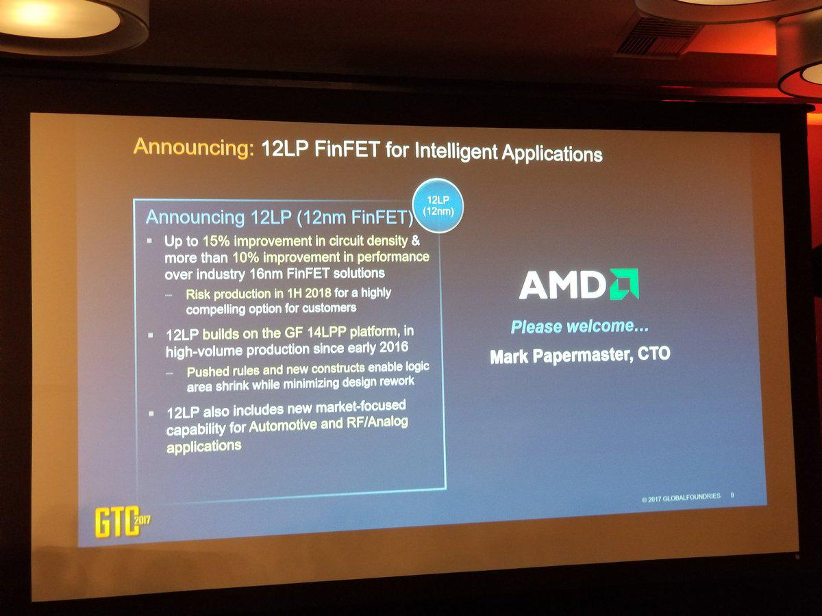
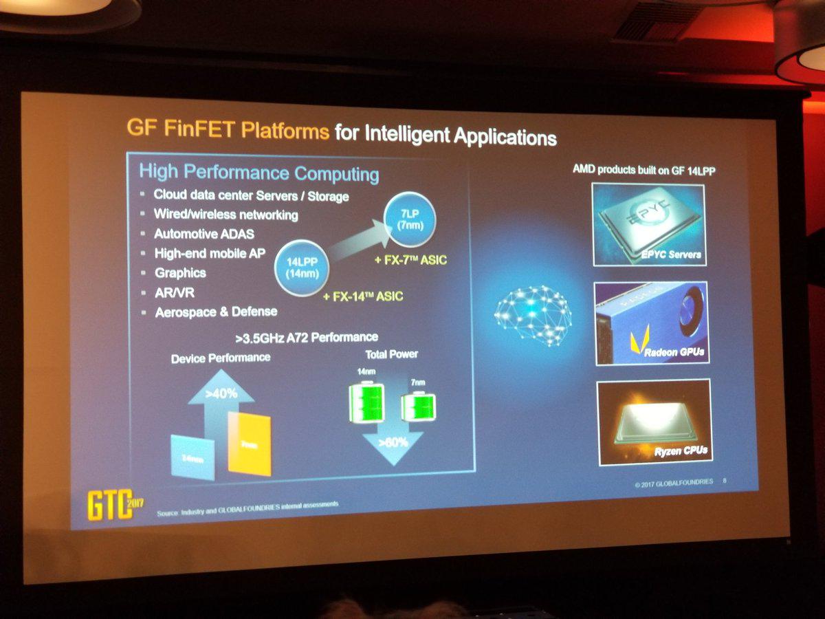
AMD’s CTO Mark Papermaster shares word that AMD will be moving from the Global Foundries 14nm LPP FinFET process to a new 12nm LP process in 2018. Global Foundries announced that 12LP will begin production in 1Q18.
The news reaches us through Toms Hardware who confirmed that the company will transition both Vega GPUs and the Ryzen line of processors to the 12nm LP process. They however are not sure if he meant that 12nm LP will be a shrink of Ryzen in 2018 and/or if Zen+/Zen 2 will also be using the 12LP process. The question rises as AMD implied that Zen 2 would use the 7nm process. The company has used both "Zen+" and "Zen 2" to refer to its next-generation die.
« Roadmap confirms quad-core Intel NUCs · AMD Moving to 12nm Vega and Ryzen in 2018
· Custom models of the Radeon RX Vega 64 Further Delayed - Vega 56 later »
icedman
Senior Member
Posts: 1067
Joined: 2013-02-22
Senior Member
Posts: 1067
Joined: 2013-02-22
#5473887 Posted on: 09/21/2017 07:12 AM
Very nice I hope they can do more with Vega being on 12nm but I doubt it'll make any noticeable difference. I can't help but feel like they would have been better off using a core with around 3000 shaders and 2 stacks hbm2 just going on gamers nexus comparisons.
JonasBeckman
Senior Member
Posts: 17329
Joined: 2009-02-25
Senior Member
Posts: 17329
Joined: 2009-02-25
#5473892 Posted on: 09/21/2017 07:28 AM
Isn't Vega already using 2 stacks of HBM2? Or perhaps you meant 4 x2 instead of the current 2 x4 design to reach the 8 GB capacity the consumer version currently has.
Shaders are a interesting one too, similar to the Fury versus Fury X GPU's there doesn't seem to be a major difference between the 64 and 56 which from my understanding of it after having read around a little bit about the subject the cards are being bottlenecked in other areas instead thus the Vega 56 when bios modded to remove some of their other limits actually do really well.
If there was a tool to allow locking and unlocking these clusters or cores it would have been really interesting to see just how far down one could take the GPU before performance was seriously impacted and how much headroom this would in turn allow for overclocking due to thermals and power usage dropping down, perhaps if disabling 8 of them (64 -> 56) gives some headroom then more could allow for the GPU to compensate by clock speed instead and perhaps see greater gains from that, eh perhaps it would hit some other limitation instead and at one point reducing these cores would start affecting performance too but there might have been some room for fine tuning things. (Perhaps later on bios modding could have some interesting possibilities depending on how things go.)
Isn't Vega already using 2 stacks of HBM2? Or perhaps you meant 4 x2 instead of the current 2 x4 design to reach the 8 GB capacity the consumer version currently has.
Shaders are a interesting one too, similar to the Fury versus Fury X GPU's there doesn't seem to be a major difference between the 64 and 56 which from my understanding of it after having read around a little bit about the subject the cards are being bottlenecked in other areas instead thus the Vega 56 when bios modded to remove some of their other limits actually do really well.

If there was a tool to allow locking and unlocking these clusters or cores it would have been really interesting to see just how far down one could take the GPU before performance was seriously impacted and how much headroom this would in turn allow for overclocking due to thermals and power usage dropping down, perhaps if disabling 8 of them (64 -> 56) gives some headroom then more could allow for the GPU to compensate by clock speed instead and perhaps see greater gains from that, eh perhaps it would hit some other limitation instead and at one point reducing these cores would start affecting performance too but there might have been some room for fine tuning things. (Perhaps later on bios modding could have some interesting possibilities depending on how things go.)
cryohellinc
Senior Member
Posts: 3348
Joined: 2014-10-20
Senior Member
Posts: 3348
Joined: 2014-10-20
#5473897 Posted on: 09/21/2017 07:46 AM
Waiting for Zen+ /Zen 2.
dfsdfs1112
Senior Member
Posts: 156
Joined: 2016-08-27
Senior Member
Posts: 156
Joined: 2016-08-27
#5473903 Posted on: 09/21/2017 08:05 AM
WHY NOT 10NM OR 7 NM
SAMSUNG HAVE IN 2018 7 NM
WHY NOT 10NM OR 7 NM
SAMSUNG HAVE IN 2018 7 NM
Click here to post a comment for this news story on the message forum.
Senior Member
Posts: 1620
Joined: 2016-01-29
Seems like 12nm lpp is an extention of 14nm lpp, much like tsmc's 12nm ffn is to 16nm ff, appears the intent is to move stuff from 14nmlpp , it specifically mentions it minimizes redesign cost from 14nmlpp.