Page 1

ECS Elitegroup Headquarters - behind the scenes
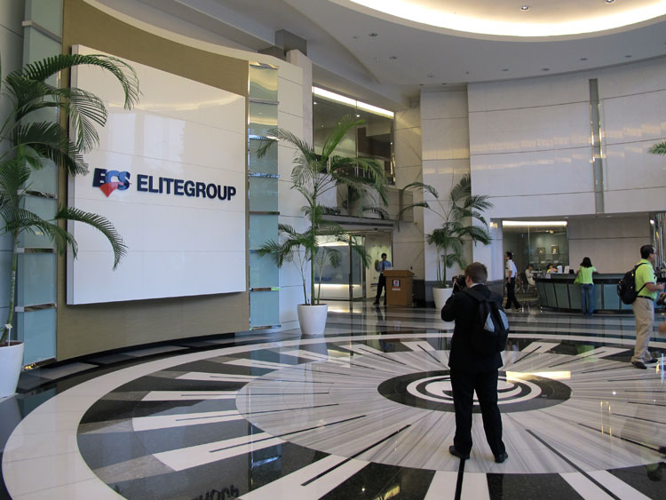
During our stay in Taiwan we had the unique opportunity to visit the ECS headquarters located in the Taipei Neihu Technology Park. Based in one of the tallest buildings in this sector the gorgeous looking and green designed building we had a sneak peak behind the scenes. ECS of course designs and manufactures desktop PCs, notebooks, servers, video cards, wireless solutions, tabs and other devices for their manufacturers and distributors worldwide. Still being an OEM predominantly provider, ECS is gaining more ground in the retail sector as well.
In this article we'll be telling you a little about the 97 meters tall building that was created in 2008. When we arrived it was poring rain, Taiwan style, outside so I do not have a proper outside building photo.
We'll show awesome building photo's but then quickly move onwards towards the Research and Development department where the good stuff is designed from PCB CAD design stages, the BIOS team and actually research and development.
We have prepared some high-definition video footage as well, showing you SMT soldering, the cubicles, some test gear on the R&D floor like temperature probing and signal processing monitoring. All in all a low tech to understand behind the scenes of ECS, with some high-end gear in the works.
Now before we dive into some photo, please have a look at the first video we took. There's no voice over (just some cool tunes) but let the imagery sink in okay ? We start at the SMT soldering station where R&D can quickly remove and attach components for quality analysis and debugging. In the last segment of the video you'll also see temperature probing on 24 channels (not all used) over a MV1000 temperature monitor. Okay, now onwards to the next page please.
