GPU Architecture
Ampere for GPU Architecture
Ampere, of course, is the base unit of electric current in the international system of units. But the GPU is named after André-Marie Ampère, a French mathematician and physicist, considered the father of electrodynamics. NVIDIA has a track record of naming their GPU architectures after mathematicians and physicists or prominent figures from closely related fields, to name a few; Pascal, Fermi, Kepler, Maxwell and, more recently, Turing. While it was no secret that the new GPUs would be based on Ampere, we've seen much discussion about fabrication nodes, architecture, and specifications. Still, everybody seems to have forgotten that Ampere already launched earlier this year for the HPC market. NVIDIA announced three Ampere based graphics cards. Shortly before announcements, specifications of the GeForce RTX 3080 and 3090 had leaked onto the web; however, it ended with a twist in Shader core counts as they doubled up from what everybody expected. These GPUs are fabricated on an 8nm node derived from Samsung. This process is a further development of Samsung's 10nm process, which means that no EUV is applied in production just yet. These cards have been announced and launched in the second half of September and, as a bit of a surprise, the GeForce RTX 3070 is arriving as well. The initial launch thus entails the GeForce RTX 3070 8GB GDDR6, RTX 3080 10GB GDDR6X, and a 24GB GDDR6X based flagship, the GeForce RTX 3090. The lineup will see Gen2 ray-tracing cores and 3rd iteration Tensor. The NVIDIA GeForce RTX 3090, as a graphics card, is going to be big on that GPU die size alright, the GA102-300-A1 GPU for example is armed with 10496 shader processors and 28 billion transistors. We know this card is to get a 20-phase power design.
GeForce RTX 3090
The products themselves then... Let us start with the flagship; the GeForce RTX 3090 comes with 24 GB of GDDR6X memory running on a 384-bit bus at 19.5 Gbps and that boils down to 936 GB/s of effective memory bandwidth. The GPU enabling it is the GA102-300 GPU, and it holds a comprehensive 10469 Shader cores. The clock frequency for the Shader cores will tick at 1695 MHz alongside a 350W TGP rating, remember, that's not a TDP. The TGP (Total Graphics Power) describes the maximum amount of graphics board power that the system power supply should be able to provide to the graphics card. The Founder editions are released at a price of $1499 USD.
GeForce RTX 3080
The GeForce RTX 3080 is based on the GA102-200 GPU and will get 8704 Shader cores clocking in at 1710 MHz. This card sees 10GB of GDDR6X memory fitted and it is running at 19 Gbps. So, that is a 320-bit bus, which is still a gnarly whopping 760 GB/s of memory bandwidth. Rated at a TGP of 320W, the card is connected with a 12-pin connector. With just these specifications, it should be as fast as the GeForce RTX 2080 Ti. The Founder editions are released at a price of $699 USD.
GeForce RTX 3070
The GeForce RTX 3070 is built around a GA104-300 GPU; it has a (still) bulky 5888 Shader cores running at 1.73 GHz. It will get 8GB of last-gen GDDR6 memory that runs at 16 Gbps on a 256-bit bus. The timeframe for release is in October as well. As we mentioned earlier, we expect an 8nm node fabrication; the card will be announced October 15th for 499 USD.
 | ||||
|---|---|---|---|---|
|
RTX 2080 Ti | RTX 3090 | RTX 3080 | RTX 3070 | |
| GPU | 12nm TU102 | 8nm GA102-300 | 8nm GA102-200 | 8nm GA104-300 |
| Transistors | 18.6 Billion | 28 Billion | 28 Billion | 17 Billion |
| Shader Cores | 4352 | 10496 | 8704 | 5888 |
| Raytracing Cores | 68 | 82 | 68 | 46 |
| Tensor Cores | 544 | 328 | 272 | 184 |
| ROPs | 96 | 96 | 96 | 96 |
| Texture Units | 272 | 328 | 272 | 184 |
| Base Clock | 1350 MHz | 1400 MHz | 1440 MHz | 1500 MHz |
| Boost Clock | 1635 MHz | 1695 MHz | 1710 MHz | 1730 MHz |
| Memory | 11GB G6 | 24GB G6X | 10GB G6X | 8GB G6 |
| Memory Clock | 14 Gbps | 19.5 Gbps | 19 Gbps | 14 Gbps |
| Memory Freq | 7000 MHz | 9750 MHz | 9500 MHz | 7000 MHz |
| Memory Bus | 352-bit | 384-bit | 320-bit | 256-bit |
| Bandwidth | 616 GB/s | 936 GB/s | 760 GB/s | 448 GB/s |
| Shader Perf TFLOP | 13.4 | 35.6 | 29.8 |
20.3 |
| RT Perf TFLOP | 110 | 285 | 283 |
163 |
| PCIe Gen | 3.0 x16 | 4.0 x16 | 4.0 x16 |
4.0 x16 |
| TGP | 320W | 350W | 320W |
220W |
| Price | $1199 | $1499 | $699 |
$499 |
| Released | Out | September 24 | September 17 |
October |
Ampere architecture has over 10000 fp32 (Shading) cores
Ampere has an updated architecture that has gotten a new SM (Streaming Multiprocessor) design. One SM is a cluster that holds your Shader processors. As most of you have noticed, the Shader processor count was a bit of an enigma; it seems that mysteriously the Shader count has doubled up from what was expected in the first place.
GA102 contains three different types of compute cores:
- Programmable Shading Cores, which consist of NVIDIA CUDA Cores, Ampere received double the Shading capabilities.
- RT Cores, which accelerate Bounding Volume Hierarchy (BVH) traversal and intersection of scene geometry during ray tracing, a gen 2 unit that now is twice as fast.
- Tensor Cores, which provide enormous speedups for AI neural network training and inferencing
The GPC is the dominant high-level hardware block with all of the key graphics processing units dwelling inside the GPC. Each GPC includes a dedicated Raster Engine, and now also includes two ROP partitions (each partition containing eight ROP units), which is a new feature for NVIDIA Ampere Architecture GA10x GPUs. The GPC includes six TPCs that each includes two SMs and one PolyMorph Engine. Each SM in GA10x GPUs then 128 Shading Cores, four third-generation Tensor Cores, a 256 KB Register File, four Texture Units, one second-generation Ray Tracing Core, and 128 KB of L1/Shared Memory, which can be configured for differing capacities depending on the needs of the compute or graphics workloads
So there would be further nuances to explain. Changes have been made to the Streaming Multiprocessor design that holds the Shading cores. The RTX 3000 series GPUs hold SMs that hold fp32 compute units. Ampere architecture supports parallel execution of FP32 and INT32 operations with independent thread scheduling. That's also described as concurrent execution of FP32 and INT32 operation. New, seen from Turing, is a combination of an INT32/FP32 cluster of Shader processors that effectively doubles up that Shader count. We'll show by example:
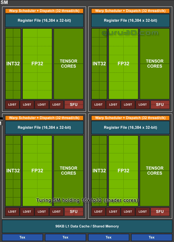
Above, the Turing SM
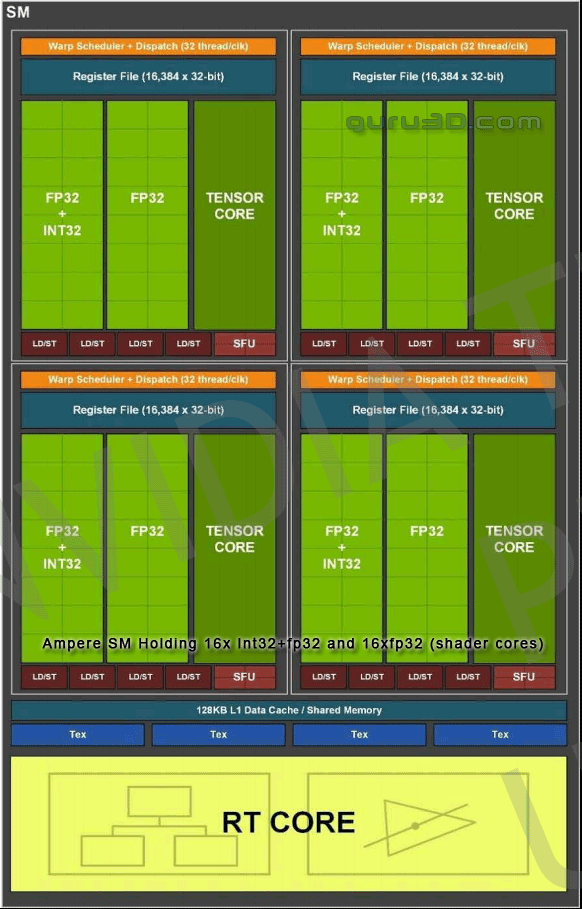
Ampere SM - Look to the left side cluster, INT32+FP32 is a significant change
The RTX 3000 series GPUs hold SMs that in their core blocks hold FP32 compute units, and that was one in the past generation as well (Turing). However, look closer. One cluster holding the INT32 is now INT32 + FP32. So to reiterate, the Ampere SM has a new datapath design for FP32 and INT32 operations. One datapath in each partition consists of 16 FP32 shader cores capable of executing 16 FP32 operations per clock. Another datapath consists of both 16 FP32 shader cores and 16 INT32 cores. And therein is the secret sauce to be found as that doubles up to twice the Shading throughput. The result of this change (compared to top Turing) is that the unit is capable of executing 32 FP32 operations per clock, or 16 FP32 and 16 INT32 operations per clock. One SM in its entirety can now execute 128 FP32 operations per clock, and that is double the FP32 rate of a Turing SM (which does 64 FP32 and 64 INT32 operations per clock). Performance gains will vary at the Shader and application level depending on the mix of instructions. According to NVIDIA, ray-tracing denoising shaders are good examples that should benefit greatly from doubling FP32 throughput. Twice the Shading performance of course can create bottlenecks all by themselves at an earlier stage in the pipeline. Therefore it has twice the shared memory and L1 cache performance for the SM, that would be 128 bytes/clock per Ampere SM versus 64 bytes/clock in Turing. Total L1 (128KB) bandwidth for GeForce RTX 3080 is 219 GB/sec versus 116 GB/sec (96KB) for GeForce RTX 2080 Super (Turing). Each segment then leads to one Tensor core and of course an RT core, both again renewed.
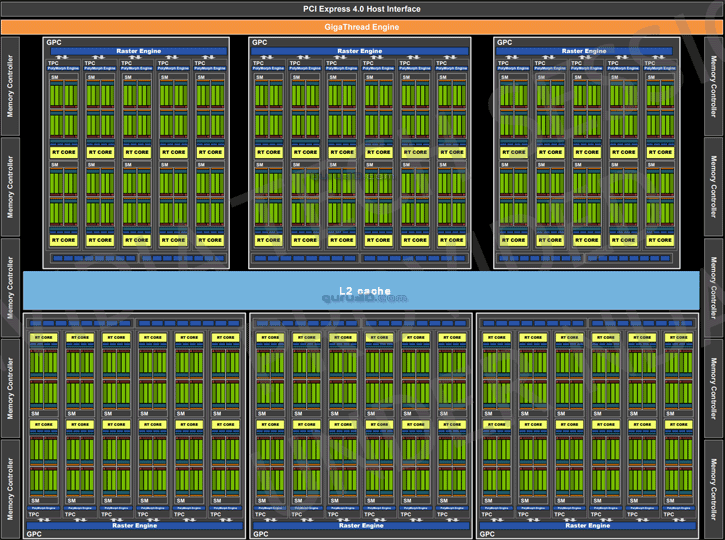
Ampere is formed based on Graphics Processing Clusters (GPCs), Texture Processing Clusters (TPCs), Streaming Multiprocessors (SMs), Raster Operators (ROPS), and later the memory controllers. The GPC is the dominant high-level hardware block with all of the key graphics processing units residing inside the GPC. Each GPC includes a dedicated Raster Engine. Ampere has one more change here, it carries two ROP partitions (each partition containing eight ROP units), which is a new feature for NVIDIA Ampere Architecture GA10x GPUs.
Up to 24GB GDDR6X Graphics memory
Worthy of a paragraph all by itself is not just the bandwidth for the RTX 3000 series but, more specifically, the memory volume for the GeForce RTX 3090. The GeForce 3080 will be released with 10GB of GDDR6X graphics memory. There is an option open for a possible 20GB version later down the line. That means the memory bus sits at 320-bits wide for the GeForce RTX 3080. The flagship GeForce RTX 3090 is going to make Flight Simulator 2020 fans happy, the mac daddy of the Ampere desktop consumer lineup gets tailored with a tremendous 24GB of GDDR6X graphics memory. And that means a 384-bit wide memory interface. GDDR6X has been announced already and can be configured in a 19 to 20 Gbps range for default configurations. And that's a big amount of memory bandwidth alright as that sits on about 1 TB/sec in effective data-rates. So if there are 12 GDDR6X ICs populated onboard, it could reach close to 1 TB/s of bandwidth (effective data-rate).
