The Zotac GeForce GTX 480
The Zotac GeForce GTX 480
So the GeForce GTX 480 has a big fat memory partition alright, 1,54 GB of GDDR5 memory which is tied to a 384-bit memory bus that binds to six memory controllers inside the GPU; six memory controllers x 64-bit = 384-bit. This memory is clocked at 924 MHz (= 3696 MHz effective).
For the GeForce GTX 470 that would be five memory controllers x 64-bit = 320-bit. The GTX 470 memory will be clocked at 837 MHz (= 3348 MHz effective).
Core frequencies then. The GeForce GTX 480 will have its core clocked at 700 MHz and its shader processors at 1400 MHz. The GeForce GTX 470 on its end will be clocked lower at 607 MHz on the core and 1215 MHz on the shader processors.
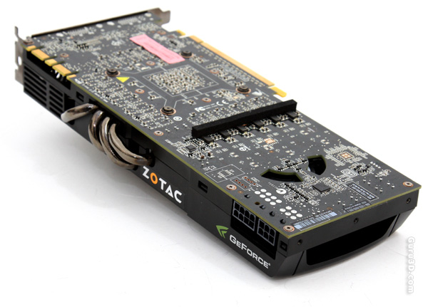
Zotacs sample that has been submitted follows reference design up-to the smallest freckle, in fact .. these are reference boards bought from NVIDIA with a Zotac sticker on them, much like any board out there currently.
| Graphics card | GeForce GTX 470 | GeForce GTX 480 |
| Fabrication node | 40nm | 40nm |
| Shader processors | 448 | 480 |
| Streaming Multiprocessors (SM) | 14 | 15 |
| Texture Units | 56 | 60 |
| ROP units | 40 | 48 |
| Graphics Clock (Core) | 607 MHz | 700 MHz |
| Shader Processor Clock | 1215 MHz | 1401 MHz |
| Memory Clock / Data rate | 837 MHz / 3348 MHz | 924 MHz / 3696 MHz |
| Graphics memory | 1280 MB | 1536 MB |
| Memory interface | 320-bit | 384-bit |
| Memory bandwidth | 134 GB/s | 177 GB/s |
| Texture Filtering rate (Bilinear) | 34 GTexels/s | 42 GTexels/s |
| Power connectors | 2x6-pin PEG | 1x6-pin PEG, 1x8-pin PEG |
| Max board power (TDP) | 215 Watts | 250 Watts |
| Recommended Power supply | 550 Watts | 600 Watts |
| GPU Thermal Threshold | 105 degrees C | 105 degrees C |
So we talked about the core clocks, specifications and memory partitions. Obviously there's a lot more to talk through. Again, for an in-depth explanation of the GF100 architecture please visit this article we wrote earlier this year.
Now, at the end of the pipeline we run into an improved ROP (Raster Operation) engine, and the GTX 480 has 48 units, the 470 has 40 for features like pixel blending and AA. There's a total of 60 texture filtering units available for the GTX 480 and with one SM less for the GTX 470; 56 texture units.
The math is simple here, each SM has four texture units tied to it.
- GeForce GTX 470 has 14 SMs X 4 Texture units = 56
- GeForce GTX 480 has 15 SMs X 4 Texture units = 60
- A fictional GeForce GTX 485 would have 16 SMs x4 TUs = 64
What's also interesting about the GTX 400 release, but was a challenge, is the move towards a smaller die and fabrication process (40nm) which often brings several advantages. One advantage is that you can insert more transistors into the silicon; as such the GF100 GPU comes with 3 billion transistors embedded into this GPU.
Despite a smaller die however, TDPs are relatively high, the GTX 480 will consume at maximum 250 Watts whereas the GTX 470 is using as much as the last generation product, roughly 225W. Still, that's definitely not as bad as the first rumors suggested.
TDP = Thermal Design Power - roughly translated, when you stress everything on the graphics card a 100% your maximum power consumption is the TDP.
The GeForce GTX 480 comes with both a 6-pin and 8-pin power connector to get enough current and a little spare for overclocking. This boils down as: 8-pin PEG = 150W + 6-pin PEG = 75W + PCIe slot = 75W is 300W available.
The GeForce GTX 470 comes with two 6-pin PEG connectors each delivering 75W and another 75W over the PCIe slot = 225W. The GeForce GTX 480 targets a price point around $449-499, while the GeForce GTX 470 is expected to be priced $299-$349.
I want to leave it at that for the physical tech side of the GPU and now move forwards to the photo shoot and other things.
