What's SATA 3 (6G)? | NAND Types
So What is NVMe?
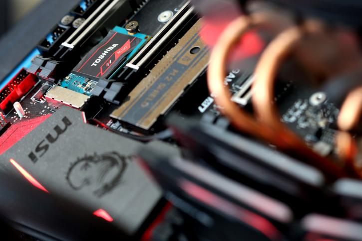
NVMe is also known as Non-Volatile Memory Express or the Non-Volatile Memory Host Controller Interface Specification. The idea behind NVMe is to improve the storage stack by optimizing the way an application accesses a Flash device. NVMe cuts corners by removing components within the I/O path like that good old-fashioned RAID controller. NVMe leverages PCIe as transport media which offers high bandwidth and a direct path to the host's CPU and memory. This, in turn, removes another potential bottleneck, the limited bandwidth of SAS or the latest SATA3 connection. NVMe makes use of your PCI-Express lanes, and as you know... the latest gen 3 PCIe lanes are fast, and thus lift the bottleneck that SATA3 has. Moving from PCIe Gen 2 to Gen 3 doubles the bandwidth available to the add-on cards installed, from 500 MB/s per lane to 1 GB/s per lane. So a Gen 3.0 PCI Express x16 slot is capable of offering 16 GB/s of bandwidth in each direction. In total that sums up to a whopping 32 GB/sec bi-directional bandwidth. Obviously, the hardware you use needs to be Gen 3.0 compatible.
Bandwidth PCI-Express PER LANE:
- PCI-Express 1.1 sends 250 MB/s per direction
- PCI-Express 2.0 sends 500 MB/s per direction
- PCI-Express 3.0 brings that number towards a whopping 1 GB/s (per lane)
So that the NVMe M.2 units use whatever they are assigned most motherboards and units now can connect on a x4 link, so a Gen 3.0 x4 link of yours can handle a total bandwidth of 8 GB/s (bi-directional) in PCIe Gen 3.0 mode, whereas the old Gen 1.0 x16 slot would be capable of 2GB/sec (bi-directional). That bandwidth combined with fast NAND and a top-notch controller can allow for massive storage speeds.
SATA 3 (6Gbps) Explained
SATA 6G (SATA 3), the latest revision of your SATA storage unit connectors, will increase the bandwidth on the SATA controller from 3 Gbit/sec to 6 Gbit/s. For a regular HDD that is not really very important. But with the tremendous rise of fast SSD drives, this really is a large plus. Typically we get 3000 Mbit/s : 8 = 375 MB/s bandwidth minus overhead, tolerances, error-correction and random occurrences. SATA 3 doubles it up, as such we get 6000 Mbit/s : 8 = 750 MB/s (again deduct overhead, tolerances, error-correction and random occurrences) of available bandwidth for your storage devices. As you can understand, with SSDs getting faster and faster that's just a much warmed and welcomed increase of bandwidth. Put SATA III in RAID and you'll have even more wicked performance at hand. Most motherboards offer only two ports per controller though, so you are (for now) limited to RAID 0 and RAID 1 (stripe or mirror).
What is NAND?
Flash memory is an electronic non-volatile computer storage medium that can be electrically erased and reprogrammed. Introduced by Toshiba in 1984, flash memory was developed from EEPROM (electrically erasable programmable read-only memory). There are two main types of flash memory, which are named after the NAND and NOR logic gates. The NAND type is primarily used in main memory, memory cards, USB flash drives, solid-state drives (those produced in 2009 or later), and similar products, for general storage and transfer of data.
NAND Types
At the beginning, memory cells stored just a single bit of information. However, the charge on the floating gate can be controlled with some level of precision, allowing the storage of more information than just 0 and 1. Based on such an assumption the MLC (Multi Level Cell) memory came to exist. To distinguish them, the old memory type was called SLC - Single Level Cell. The decision of choosing between SLC and MLC is driven by many factors such as memory performance, the number of target erase/program cycles and level of data reliability. The MLC memory endurance is significantly lower (around 10,000 erase/program cycles) compared to SLC endurance (around 100,000 erase/program cycles).
Toggle-mode MLC - Toggle-mode MLC is asynchronous NAND that is supposed to provide similar performance as synchronous NAND, but at a lower price. Independent testing has not verified these claims yet. Toggle-mode MLC is also known as double-data-rate asynchronous NAND.
Synchronous and asynchronous NAND, based on spec sheets, look remarkably similar in performance. However, they aren't. Synchronous NAND is more expensive than asynchronous. Sync NAND is used when performance is everything, such as with gaming systems.
TLC flash memory (triple-level cell flash) is a type of solid-state NAND flash memory that stores three bits of data per cell of flash media. TLC flash is less expensive than single-level cell (SLC) and multi-level cell (MLC) solid-state flash memory, which makes it appealing for consumer devices that use solid-state storage. The drawbacks to using TLC flash are performance, reliability, and longevity. TLC flash will also have lower write endurance than both SLC and MLC flash. Generally, the more bits of data the cell has, the fewer write cycles it will support. SLC memory cells can withstand up to 100,000 write cycles before failing. A 2-bit MLC memory cell can typically withstand up to 10,000 write cycles before failing. A TLC memory cell can sustain about 1,000 write cycles before failing, which is why thus far it has been limited to consumer-grade applications.
Vertical (3D) V-NAND is physical vertical NAND cell stacking not to be puzzled with chip stacking in a multi-chip package. In 3D NAND, NAND layers, not chips, are stacked in a single IC. Stacking cells vertically has several benefits: it provides a higher capacity/volume ratio in a smaller physical space and improves electrical performance by shortening the interconnect length between cells (which also reduces power consumption). The good news is continued cost reduction, smaller die sizes and more capacity per NAND chip. Also, installed NAND toolsets in the wafer fabs can, for the most part, be reused, thereby extending the useful life of fab equipment.
So What About That New Smaller NAND Lifespan?
New <= 25nm NAND FLASH memory was introduced, designed to be cheaper. The overall lifespan of the ICs has been reduced from 10,000 towards 5,000 program/erase cycles. Rumors are, that the numbers for consumer grade 20/25nm NAND flash memory (as used on the SSD tested today) are even lower at 3,000 program/erase cycles. But granted, as drastic as that sounds, it's all relative as this lifespan will very likely last longer than any mechanical HDD. Drive wearing protection and careful usage will help you out greatly. With an SSD filled normally and very heavy writing/usage of say 10 GBs data each day 365 days a year, you'd be looking at roughly 22 full SSD write cycles per year, out of the 3,000 (worst case scenario) available. However, all calculations on this matter are debatable and theoretical as usage differs and even things like how much free space you leave on your SSD can affect the drive.


