
Architecture and Chiplet Design
Chiplet Design & Architecture
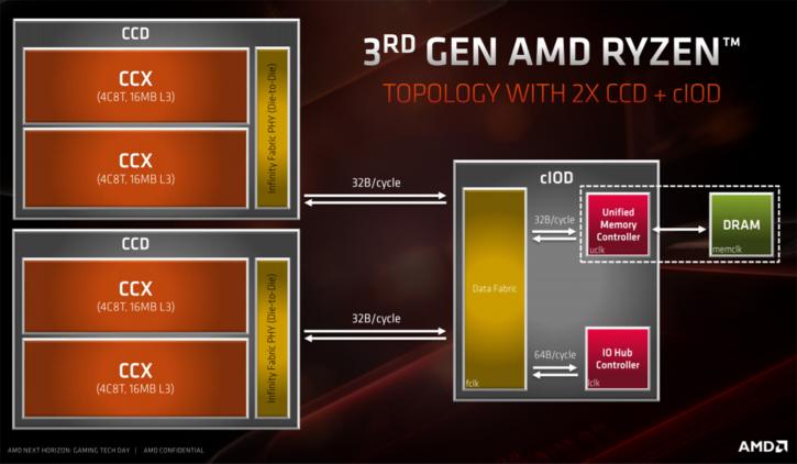
I’ve mentioned this in the review already, but also explained multiple times that AMD is now effectively moving towards a chiplet design starting with Ryzen 3000 aka ZEN2. Multi-die chips, thus multiple chips in one package is what we're talking about when we refer towards a chiplet design, it’s one of the many answers to be able to fight off Moore's Law, now and in the future. AMD already is using the technology to connect multiple processors in Threadripper and for servers, Epyc, but also Intel with Kaby Lake-G. However new in the evolution of processors are chiplets, these are multiples of chips stacked together on an interposer that form the actual chip. Chiplets for AMD Ryzen 3000, Zen 2 features a 14nm I/O die along with 7nm CPU chiplets (each holding eight cores per die) (for EPYC2 and Ryzen 3000). AMD has mentioned that this process will bring great value. AMD is updating its Infinity Fabric that connects the different dies that hold the cores. Current Epyc, Ryzen and Threadripper CPUs all are connected via the Infinity Fabric. With the Zen 2 architecture, AMD places one I/O die chip that sits in the middle, which is connected to two 8-core dies. These AMD CPU chiplets are connected with the 2nd gen generation Infinity Fabric. The I/O chip (the bigger one) is fabbed at 14nm process, the CPU cores (two) on 7nm, upcoming EPYC chips will include multiple Zen 2 CPU modules. An interesting addition, in theory, it supports eight DDR DRAM interfaces.
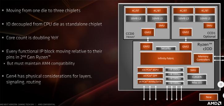
One of the bigger issues at hand when manufacturing large monolithic CPU/GPU dies is that yields decrease and costs go up. As you create larger products, that is an issue. So why not combine multiple dies onto one merged package? In an example, as posted in a paper (below) you can see four GPUs with a CPU partition combined into one chip. The data is then moved via an interposer, sending the right data to the right place. Researchers have been developing this concept called “chiplets” with the idea that it will let data move faster and freer to make smaller, cheaper, and more tightly integrated computer systems. The idea is that individual CPUs, memory, and other key systems can all be mounted onto a relatively large slice of silicon, called an active interposer, which is thick with interconnects and routing circuits. AMD now is offering the very first chiplet design. The chip holds one or two 7nm 8–core dies which are connected to the IO chip.
Now below are a few shots of the new Gen3 architecture, I want to disclose that we'll be going in-depth with these in the final review. But with these rushed articles it's sometimes better to step back.
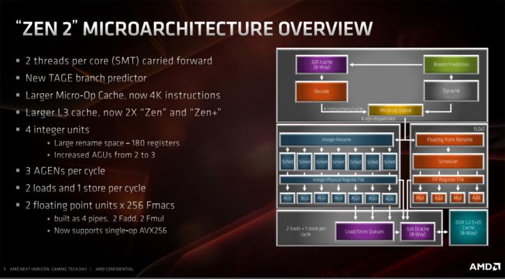
Zen 2 architecture is an advancement Zen, and Zen had some bottlenecks to be dealt with. These are solved in this design and at the same time, thanks to the smaller 7nm transistors, added extra functionality in important places. The image above shows the block diagram of the Zen 2 core. There is a new branch predictor, a larger micro-op cache, an additional address generation unit and a new floating point unit, which can handle 256-bit at the same time. Oh and that and more L3 cache which was doubled up from last gen.
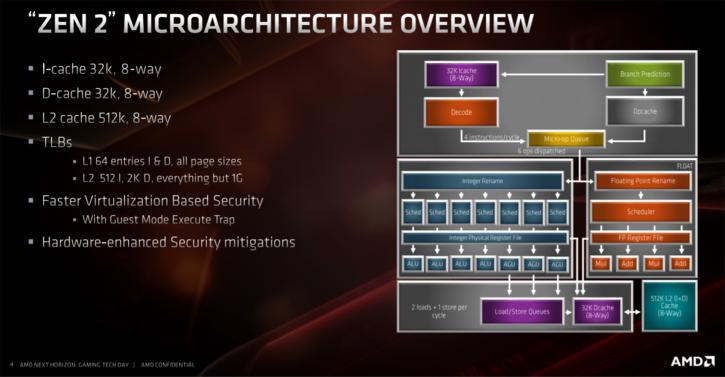
Increasing the cache is costly, and of course, takes more transistors, that is where 7nm helps them out greatly. However, AMD also reduced the L1 instruction cache from 64 kB to 32 kB. The instruction cache contains the x86 instructions that were retrieved from the memory for processing. However, by giving this cache more inputs and outputs ( 8-way associative instead of 4-way associative). Improving algorithms for pre-fetching instructions as clever as possible and by increasing the caches at other levels (like the L3 cache), the effect of the smaller instruction cache is limited, at least that's what AMD states. Once our reviews go live well talk a bit more about this. L1 data cache was 32 kB at Zen and remained that at Zen 2. Also unchanged is the L2 cache, which is still 512 kB per core. The L3 cache, however, is shared by the cores and that one has doubled. Four cores are partitioned together in a group called a core complex (CCX). The last gen had MB L3 cache with previous Zen processors, this has been doubled to a whopping 16 MB L3 cache.
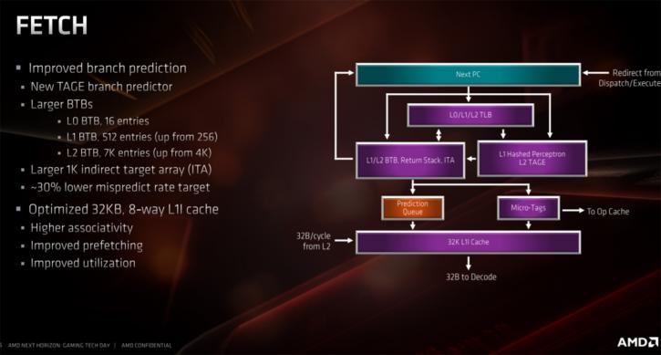
Some pointers though, Ryzen Gen 3 has improved branch prediction / better instruction prefetching, a re-optimized Instruction cache and a larger op cache. Floating point performance has effectively doubled with much more cache, L3 cache – L2 512KB / L3 Slice 4MB. New support for AVX 256 (single cycle) is included as well. At the front-end of the processor, a new innovation a new branch predictor, which works according on what is called the TAGE methodology. Studies have indicated that such a predictor offers the better of not best results. Also, an important adjustment is to double the size of the micro-op cache to 4000 instructions.
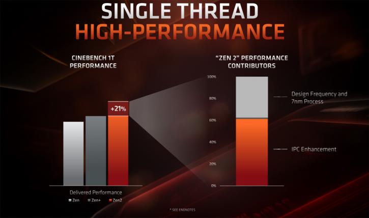
All these things lead to faster IPC which is what AMD has been hunting down hard. We cannot wait to actually test the perf on that. Obviously, there have been a number of other changes, with the chiplet design the Infinity fabric is updated not at its 2nd generation. We'll talk more about that in the final reviews.
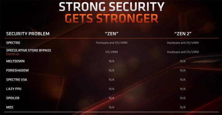
What I also wanted to share for now is that AMD has further secured their procs in hardware, there is CPU hardening for Spectre exploits built into the processor, which is awesome new.
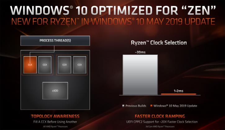
AMD has been working closely with Microsoft to improve multi-threading. With the May 2019 update, you’re going to see improvements as it has been implemented in there.
