
The Vega Lineup specifications
The Vega Lineup specifications
The cheapest model is the Radeon RX Vega 56 which will offer 10.5 TFLOPS of fp32 performance at a price of 399 USD. All three cards have been fitted with 8GB of HBM2 graphics memory, two stacks thus with a 2048-bit memory bus. The 64 editions will offer 484 GB/s of bandwidth, the 56 shader cluster edition get 410 GB/s of graphics memory bandwidth. So when we break down the products in a more simplistic way at the product we see the following. The 399 USD air-cooled Radeon RX Vega 56 card will get the following clocks:
- 1,156 MHz base clock
- 1,471 MHz boost clock
- 10.5 TFLOPS game precision performance.
- TBP: 210 Watt
The 499 USD air-cooled Radeon RX Vega 64 card will get the following clocks:
- 1,247 MHz
- 1,546 MHz
- 12.66 TFLOPS game precision performance.
- TBP: 295 Watt
The 699 USD liquid-cooled Radeon RX Vega 64 card will get the following clocks:
- 1,406 MHz
- 1,546 MHz
- 13.7 TFLOPS game precision performance.
- TBP: 345 Watt
Radeon RX Vega 64 - Liquid cooled edition
A lot has been said and spoken regarding this graphics card series. So give or take the model of your choice, Radeon RX Vega will offer you a comfortable ~12.5 TFLOP of single precision (fp32) game performance. You guys have seen all rumors, leaked benchmarks and FE edition results. While we have yet to test performance, we feel that the product will battle the reference clocked GeForce GTX 1080, which offers 9 TFLOPs and the GeForce GTX 1080 Ti (Pascal) at roughly 11 TFLOPS. This means that AMD can position itself at a rather comfortable position in the PC gaming domain. Time will tell, well the review will.
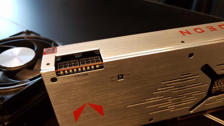
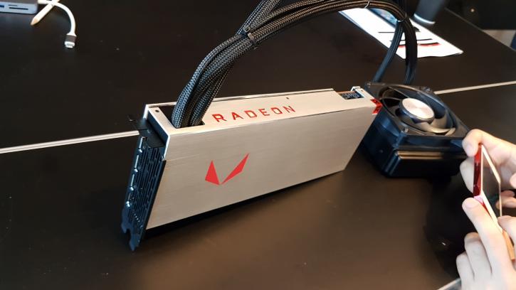
Radeon RX Vega 64 LCS comes with two 8-pin PCIe power connector and GPU power phase LED light activity. All in a nice silver / alu design cover. The fan and radiator size is 120mm.
The board partners will offer their own revision of Radeon RX Vega with customized PCBs, factory tweaks and efficient cooling solutions. These will become available in Q3 of 2017. BTW in the upper photo you can see the dual-BIOS switch that will be on all vega cards. There will be energy efficiency choices be made for the secondary BIOS. We'll talk a bit more about that once we can actually review these cards.
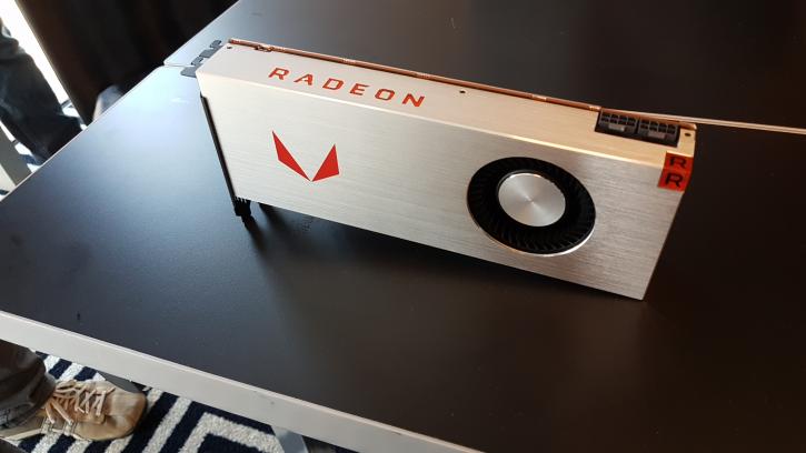
The Radeon RX Vega 64
A little deeper into the GPU
For the Radeon RX Vega 64 - 64 shader clusters with 64 shader per cluster is 4096 shader processors that turbos towards the 1.545 GHz dynamic clock frequency. The Vega 10 GPU is based on a whopping 12.5 billion transistors and is fabbed on a 14nm FinFET LPP process. It comes with over 45MB of SRAM cache across the chip and thus holds either an 8GB (consumer) or 16 GB (Pro) configuration. While we'll get into the details of Vega in our review, the GPU is based on a design with 4 synchronous compute pipes, four next gen geometry engines and for the fully activated SKU, 64 next gen compute units will get you 4096 Shaders processors and 56 x 64 = 3584 shader procs for the 56 model. The full 64 model would be tied towards 64 ROPs and 256 / 224 Texture memory units. G33k stuff: L2 cache has been doubled to 4 MB. Render back-ends are now clients of the L2. So basically, the Vega GPU is based on 64 shader clusters with 64 shader processors each. So that makes a nice 4096 shader processors in total. These shader partitions are tied to 64 ROPs. TMUs wise for a fully enabled unit AMD has always used a 4:1 ratio meaning 64 CUs x 4 = 256 texture units, which is a good number. Memory sits on a 2048-bit wide bus (two memory stacks of 1024-bit each) spread over the 64-bit controllers. Vega is fitted with HBM2 (vertically stacked graphics memory placed on die) memory as well as a using a new IO gateway, the graphics memory cache is synonym for High Bandwidth Cache. Earlier on AMD stated that Vega is a GPU with 200 new features. A number of things are key for AMD with this scalable GPU new architecture.
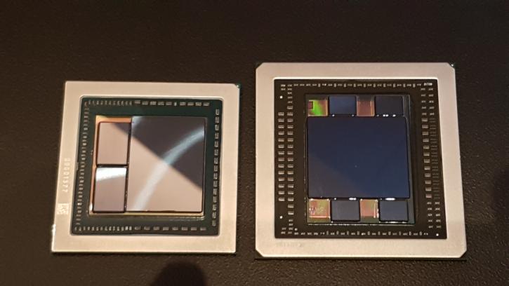
To the left the new Vega 10 GPU with two 4GB HBM2 stacks - to the Right the older Fiji GPU (Fury) holding four 1 GB stacks
Vega 10 is using High Bandwidth Video Memory, VRAM, graphics memory or whatever you like to call it. The specific type type used is HBM2 memory. The graphics engineers from AMD claimed that HBM2 will offer you 5x the power efficiency compared to any other graphics memory including GDDR5, and yes that is huge. Another benefit obviously is capacity. HBM is on-chip vertically stacked (slabs of memory cells placed on top of each other) and you know it, when it comes to caches and memory bigger is simply better (in terms of storage volume). With the second iteration of HBM, HBM2 AMD now has 8x the density per stack with a 50% smaller footprint.
