Product Showcase
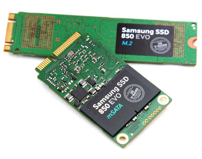
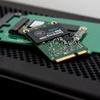
Well, here we are. These storage units make use of Samsung's own MLC 3D-V-NAND. I do wish though that manufacturers would go with a black PCB. The M.2 unit has only two NAND flash memory ICs on the PCB for the entire 120GB. That is going to hurt write performance, a 250GB or higher model would not have that issue though. The 1TB mSATA version uses four NAND ICs.
Below the stickers there is the MGX controller. This is a multi-controller with the ability of a possible 175 MB/s to 200 MB/s per channel throughput. The NAND FLASH partitions are assigned directly to the controller. The PCB also holds a DDR3 memory cache chip from Samsung. This functions as a hot data buffer.
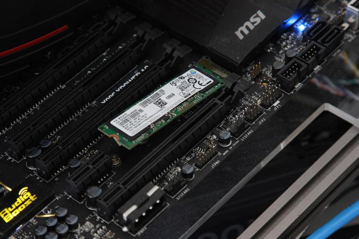
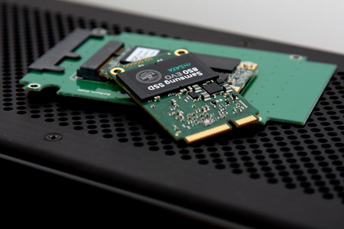
As stated, the NAND used is the new 3D V-NAND in architecture where memory cells are stacked and this way they can put more of them in a single chip. These ICs are based on 32 layer 3D V-NAND. An interesting fact is that the power consumption of the Samsung SSD is extraordinary low with an IDLE rating of 2 Milli-watts and roughly 4 Watts when active. We can see these SSDs ending up in both notebooks and PCs. Above, an example of the M.2 slot with the M.2 unit, we still need to screw it in securely here of course.
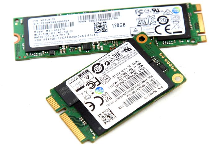
Very few NAND ICs, in total on both sides you will count four of them. That is the trick with 32 layer 3D V-NAND, they can stack cells and thus have less chips to produce. Less components needed equals a cheaper to produce product. In the background you can see a SATA3 adapter board onto which we will mount the mSATA unit to test.
