AMD's Radeon series 4800 chipset
AMD's Radeon series 4800 chipset
As you guys know by now ATI's Radeon HD 4850/4870 are both using the same GPU (graphics processor). The codename for these chips (ASIC) is RV770. The Radeon HD 4890 uses the RV790 GPU. Honestly, we feel it's the exact same GPU yet a better yielded version which can take a slightly higher voltage and clock much higher.
AMD put nearly a billion transistors into the GPU, it is still built upon a 55nm (260 mm2 Die size) production, and not 40nm as rumored earlier. The chip is 16 mm wide and high. Actually quite large, for a 55nm product.
Being based off that RV770 graphics processor the Radeon 4890 series graphics processors also have 800 scalar processors and forty texture units (16 in last-gen architecture). The stream/compute/shader processors (can we please just name them all shader processors?) definitely had a good number of changes; if you are into this geek talk, you'll spot 10 SIMD clusters each carrying 80 32-bit Shader processors (this accumulates to 800). If I remember correctly, one SIMD unit can handle double precision.
Much like the NVIDIA GTX 200 architecture, the scalar stream processors per SIMD unit have 16KB of local data cache/buffer that is shared among the shader processors. Next to the hefty shader processor increase you probably already notice the massive amount of texture units. In the last generation product we noticed 16 units, the 4800 series has 40 units.
It's a bit inaccurate to do but divide the number of ATI's scalar shader processors with the number 5 and you'll roughly equal the performance to NVIDIA's stream processor. You could (in an abstract way) say that the 4800 series have 160 shader units, if that helps you compare it towards NVIDIA's scaling. Again there's nothing scientific or objective about that explanation.
Anyhow. With 800 shader processors combined with some new higher clock frequencies it can produce the raw power of 1360 GigaFLOPs in simple precision. Well, depending on how that is measured of course.
Let's make a comparison chart for you to understand the differences between the Radeon HD 4870 and 4890:
|
|
ATI Radeon |
ATI Radeon |
ATI Radeon |
|
# of transistors |
956 million |
956 million |
959 million |
|
Stream Processing Units |
800 |
800 |
800 |
|
Clock speed |
625 MHz |
750 MHz |
850 (and higher) |
|
Memory Clock |
1980 MHz (effective) |
3600 MHz (effective) |
3900 MHz (effective) |
|
Math processing rate (Multiply Add) |
1000 GigaFLOPS |
1200 GigaFLOPS |
1360 GigaFLOPS |
|
Texture Units |
40 |
40 |
40 |
|
Render back-ends |
16 |
16 |
16 |
|
Memory & type |
512MB GDDR3 |
512/1024MB GDDR5 |
1024MB GDDR5 |
|
Memory Bandwith |
64 GB/s |
115 GB/s |
125 GB/s |
|
Memory interface |
256-bit |
256-bit |
256-bit |
|
Fabrication process |
55nm |
55nm |
55nm |
|
Power Consumption (peak) |
110W |
160W |
190W |
|
Power Consumption (Idle) |
30W |
90W |
60W |
So comparing apples to apples, the Radeon HD 4890 simply put is a faster clocked product, a graphics update. The core GPU frequency will be clocked 100 MHz faster at minimum (some board partners will clock at 900 MHz), and then there's an increase of the GDDR5 memory clock giving the product ~125 GB/s of framebuffer bandwidth.
Two SKUs
So to understand what ATI is releasing, please understand this: there will be two SKUs (products) based off the 4890 released:
-
Radeon HD 4890 Standard (reference) version
-
Radeon HD 4890 OC editions -- At least 900 Mhz Core frequency and 3900+ MHz Memory clocks
The reference based products will all have 1024MB of graphics memory, ATI does not rule out that IAB/AIC partners will bring a 512MB version to the market as well. Good to know is that the card is designed in such a way you can clock it to 900 ~ 1000 MHz on the fly. We'll of course check that out in our overclock session. The Radeon HD 4980 will be introduced at a 269 USD MSRP price tag.
Anyway, let us have a peek at the product with the help of a photo-shoot.
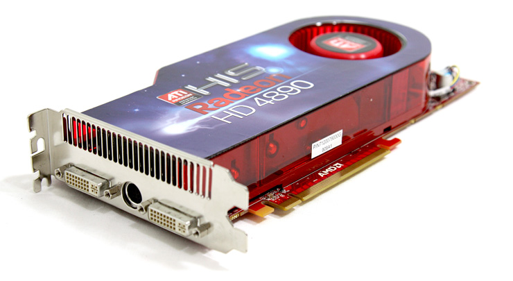 We'll be testing the HIS Technology Radeon HD 4890 edition today.
