Product Innards
Product Innards
So, we take off the back-plate locked in with screws. At the backside there is a gap between the components and back-plate through the use of riser standoffs. Let's immediately zoom in at the GPU front-side, as that's the sugah-shot right there. The GPU is extensively greased with TIM, and it looks we got the silicon molded version.
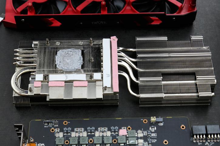
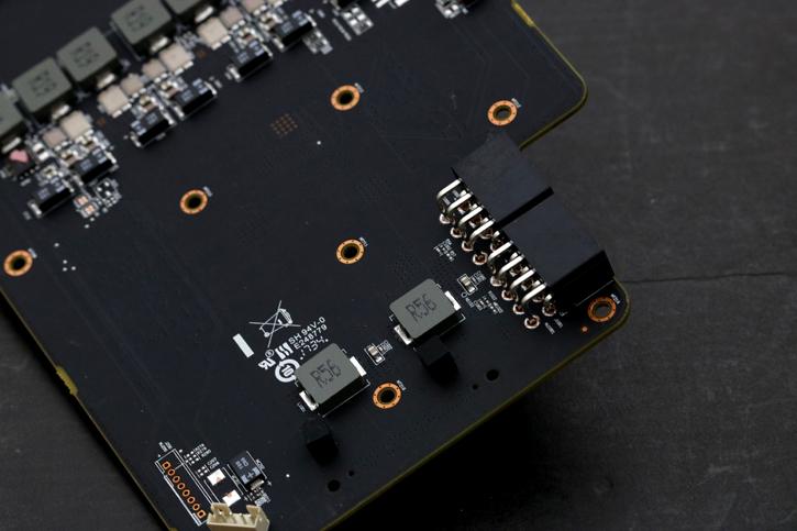
The cooling solution, it uses heat-pipes that pass through the traditional block, with thermal paste tied to the all-copper yet nickel plated block. That's as good as it gets really. When we flip the PCB around you can also see that the critical components are covered with a full contact plate (padding underneath as well). The power stages have padding and thus is cooled as well as most ICs.
Reference Radeon RX Vega 56/64
Red Devil Vega 56 PCB
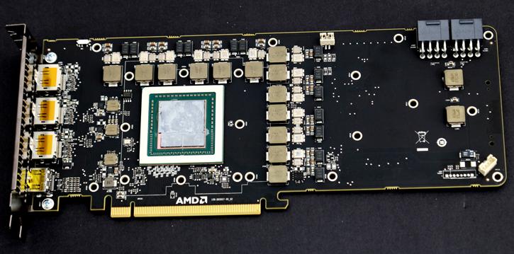
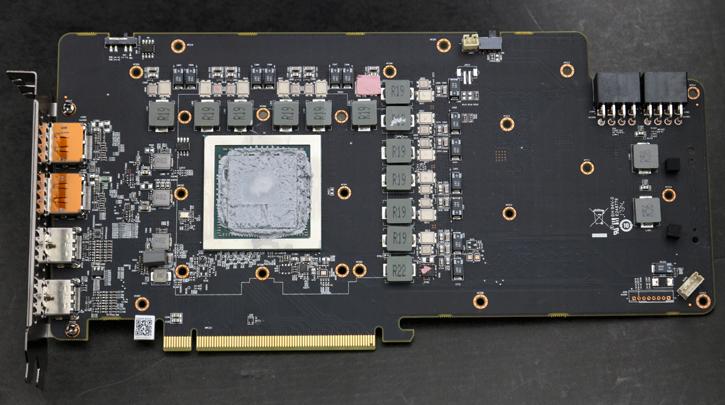
With the cooler removed, we now have the full PCB and all components visible. This is a very clean PCB design alright, that right side is hardly used other than to provide a more sturdy design for the cooler. As you can see, the DNA of the Red Devil shares 98% of the reference design.
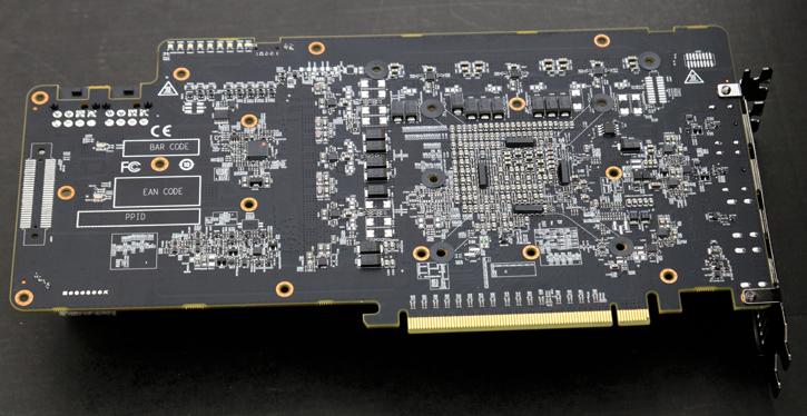
The backside is crowded and, to the left, you can see the voltage regulator, the board design stays incredibly close to reference really - but let's run through some of the components.
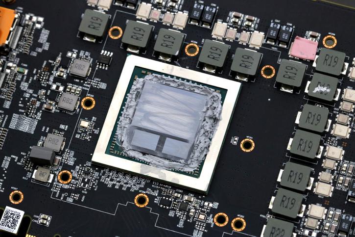
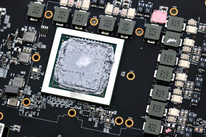
First and foremost, here we have the Vega 10 graphics processor from AMD. I removed the thermal compound a bit, but the readout was washed as you can see. As mentioned, the PCB and GPU design should be the same for both the 56 and 64 models btw. At the lower GPU side, you can see the two HBM2 stacks, each 4GB. We have the 'closed' mold version of the GPU. A hefty amount of TIM was applied, so the HBM2 stacks can cool alongside the base plate a bit as well.
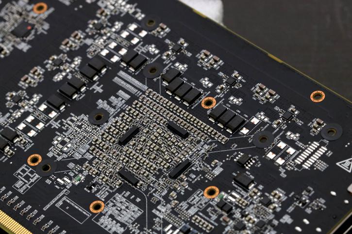
So in the above photo, you can see the opposing backside of the GPU, it shows many, really many ceramic capacitors.
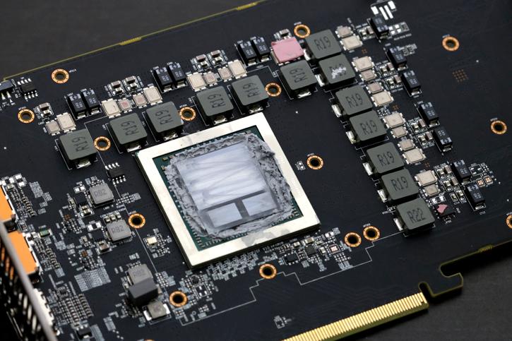
The card uses solid capacitors that are surrounding the GPU socket. We'll look at the voltage regulator in a second as well. No memory leaves open opportunities in terms of placement on the PCB. As such, you can see the voltage regulators are located at what normally would be the location of the memory ICs.
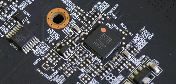
The reference design uses an International Rectifier IR35217 power controller, a fairy undocumented 8-channel multi-phase controller that can provide six phases for the GPU and another two for, say, memory. If you look at the previous image you'll notice PowerColor is doubling GPU phases up, they, in fact, use phase doublers located on the backside of the PCB. This is common on many graphics cards. So it's 6 phases but doubled up to 12, ergo why PowerColor denotes this as 12-phase power delivery.