The Turing GPU
Turing GPU Architecture
We'll talk you through the new Turing architecture in the next chapters, we'll begin a bit more low-level, a more generic to understand of an explanation what Turing is all about, followed by paragraphs at a deeper level of understanding. It's been a long time coming but NVIDIA has announced their new consumer graphics cards, the GeForce RTX series. When we crawl back towards February 2018 I posted a news-item, Reuters mentioned a new codename that was not present on any of NVIDIAs roadmaps, Turing. And that was a pivotal point really, but also added some confusion. Turing is a name more related and better fitted to AI products (the Turing test for artificial intelligence). In case you had not noticed, look at this: Tesla, Kepler, Maxwell, Fermi, Pascal, Volta. Here is your main hint to be found. Historically Nvidia has been naming their architectures after famous scientists, mathematicians, and physicist. Turing, however, sounded somewhat more plausible than Ampere, who was a physicist.
Alan Turing
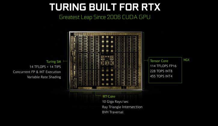
Alan Turing is famous for his hypothetical machine and the Turing test, the machine can simulate any computer algorithm, no matter how complicated it is. That test is applied these days to see if an AI is, in fact, intelligent at a conscious level. At this point I like to point you towards the beautiful movie Ex Machina, the entire movie could have been named the Turing test. The idea was that a computer could be said to "think" if a human interrogator could not tell it apart, through conversation, from a human being. In the paper, Turing suggested that rather than building a program to simulate the adult mind, it would be better rather produce a simpler one to simulate a child's mind and then to subject it to a course of education. A reversed form of the Turing test is actually widely used on the Internet; the CAPTCHA test is intended to determine whether the user is a human or a computer. That test, my friends, he designed in 1950. During WW2 Turing also has been leading Hut 8, the section which was responsible for German naval cryptanalysis. He devised a number of techniques for speeding the breaking of German ciphers, including improvements to the pre-war Polish bombe method, an electromechanical machine that could find settings for the Enigma machine. He has had a big role in cracking intercepted coded messages that enabled the Allies to defeat the Nazis in many crucial engagements, including the Battle of the Atlantic. Back to graphics processors though. Back in June 2018 NVIDIA posted a tweet congratulating and celebrating the birth date of Alan Turing. That was the point where I realized, at least one of the new architectures would be call Turing. All the hints lead up towards Siggraph 2018, last Monday NVIDIA made an announcement of a new professional GPUs, called ... Quadro RTX 8000, 6000, 5000 and the GPU empowering them is Turing. The graphics architecture called Turing is new. It’s a notch of Pascal (shader processors for gaming), it’s a bit Volta (Tensor cores for AI and deep learning) and more. Turing has it all, the fastest fully enabled GPU (GU102) presented has 4608 shader processors paired with 576 Tensor cores. What’s new however are the addition of RT cores. I would love to call them RivaTuner cores (pardon the pun), however, these obviously are Ray tracing cores. Meaning that NVIDIA now has added core logic to speed up certain ray tracing processes. What is that important? Well, in games if you can speed up certain techniques that normally take hours to render, you can achieve greater image quality.
The Turing GPU (TU102)
Looking at the Turing GPU, there is a lot of stuff you can recognize, but there certainly have been fundamental block changes in the architecture, the SM (Streaming Multiprocessor) clusters have separated, core separated isolated blocks, something the Volta GPU architecture also shows as familiarity. Mind you that the base building block for all Turing GPUs will be the GU102, that is the flagship GPU that will be used on the GeForce RTX 2080 Ti. The TU102 is the GPU / graphics processor used on the GeForce (gosh I really have the tendency to write GTX nearly automatically when typing this article) RTX 2080. So the GU104 is a more simplified revision of the GU102, but shares the very same architecture.
Turing GPU Specifications
Turing, and allow me to take the GPU TU102 as the primary example, is massive, it counts 18.6 billion transistors localized onto a 754mm2 die. In comparison, Pascal had close to 12 billion transistors on a die size of 471mm2. Gamers will immediately look at the shader processors, the Quadro RTX 8000 has 4608 of them enabled and since everything with bits is in multitudes of eight and while looking at the GPU die photos; it has 72 SMs (streaming multiprocessors) each holding 64 cores = 4608 Shader processors. This means A fully enabled GPU has 576 Tensor cores, 36 Geometry units, and 96 ROP units. This GPU is fabbed on an optimized 12nm TSMC FinFET+ node. We've placed the main specifications in a table overview.
|
| ||||||
|---|---|---|---|---|---|---|
| GeForce | RTX 2080 Ti FE | RTX 2080 Ti | RTX 2080 FE | RTX 2080 | RTX 2070 FE | RTX 2070 |
| GPU | TU102 | TU102 | TU104 | TU104 | TU106 | TU106 |
| Node | TSMC 12 nm FFN | |||||
| Die Size mm² | 754 | 545 | 445 | |||
| Shader cores | 4352 | 4352 | 2944 | 2944 | 2304 | 2304 |
| Transistor count | 18.6 Billion | 18.6 Billion | 13.6 Billion | 13.6 Billion | 10.8 Billion | 10.8 Billion |
| Base frequency | 1350 MHz | 1350 MHz | 1515 MHz | 1515 MHz | 1410 MHz | 1410 MHz |
| Boost frequency | 1635 MHz | 1545 MHz | 1800 MHz | 1710 MHz | 1710 MHz | 1620 MHz |
| Memory | 11GB GDDR6 | 11GB GDDR6 | 8GB GDDR6 | 8GB GDDR6 | 8GB GDDR6 | 8GB GDDR6 |
| Memory frequency | 14 Gbps | 14 Gbps | 14 Gbps | 14 Gbps | 14 Gbps | 14 Gbps |
| Memory bus | 352-bit | 352-bit | 256-bit | 256-bit | 256-bit | 256-bit |
| Memory bandwidth | 616 GB/s | 616 GB/s | 448 GB/s | 448 GB/s | 448 GB/s | 448 GB/s |
| L2 Cache | 5632 KB | 5632 KB | 4096 KB | 4096 KB | 4096 KB | 4096 KB |
| RT cores | 68 | 68 | 46 | 46 | 36 | 36 |
| Tensor cores | 544 | 544 | 368 | 368 | 288 | 288 |
| Texture units | 272 | 272 | 184 | 184 | 144 | 144 |
| ROPs | 96 | 96 | 64 | 64 | 64 | 64 |
| TDP | 260W | 250W | 225W | 215W | 185W | 175W |
| Power connector | 2x 8-pin | 2x 8-pin | 8+6-pin | 8+6-pin | 8-pin | 8-pin |
| NVLink | Yes | Yes | Yes | Yes | - | - |
| Performance (RTX Ops) | 78T RTX-Ops | 60T RTX-Ops | 45T RTX-Ops | |||
| Performance (RT) | 10 Gigarays/s | 8 Gigarays/s | 6 Gigarays/s | |||
| TFlops fp32 | 14.2 / 13.4 | 10.6 / 10 | 7.9 / 7.5 | |||
| Max Therm degree C | 89 | 89 | 89 | |||
| price | $ 1199 | $ 999 | $ 799 | $ 699 | $ 599 | $ 499 |
Deeper level architecture
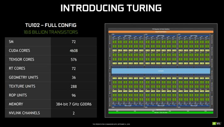
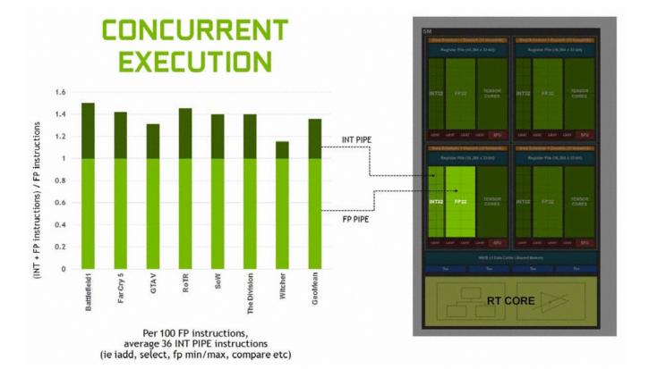
We'll try and be brief here, but Turing is a new and completely overhauled architecture that actually has gotten a new SM (Streaming multiprocessor) design. As I mentioned it has a bit of everything, but mostly it hints towards Volta. Two SMs are included per TPC (= Texture / Processor Cluster - a group made up of several SMs). Each SM has a total of 64 FP32 Cores and 64 INT32 Cores. Now before you get all confused yes that is radically different from Pascal (GeForce series 1000)who have one SM per TPC and 128 FP32 Cores per SM. The Turing SM architecture supports parallel execution of FP32 and INT32 operations, independent thread scheduling similar to the Volta GV100 GPU. That's also described as concurrent execution of FP32 and INT32 operation. Each Turing SM holds eight Turing Tensor Cores. With that out of the way, have a peek at the block diagram below.
Each Turing SM is partitioned into four processing blocks, each holds 16 FP32 Cores, 16 INT32 Cores, two Tensor Cores, one warp scheduler, and one dispatch unit. Each block includes a new L0 instruction cache and a 64 KB register file. The four processing blocks share a combined 96 KB L1 data cache/shared memory. Traditional graphics workloads partition the 96 KB L1/shared memory as 64 KB of dedicated graphics shader RAM and 32 KB for texture cache and register file spill area. Compute workloads can divide the 96 KB into 32 KB shared memory and 64 KB L1 cache, or 64 KB shared memory and 32 KB L1 cache.
Concurrent Execution of Floating Point (fp32) and Integer Instructions (int32)
Turing’s SM initiates a new unified architecture for shared memory, L1, and texture caching. This unified design allows the L1 cache to leverage resources, increasing its hit bandwidth by 2x per TPC compared to Pascal, and allows it to be reconfigured to grow larger when shared memory allocations are not using all the shared memory capacity. The Turing L1 can be as large as 64 KB in size, combined with a 32 KB per SM shared memory allocation, or it can reduce to 32 KB, allowing 64 KB of allocation to be used for shared memory. Turing’s L2 cache capacity has also been increased. Combining the L1 data cache with the shared memory reduces latency and provides higher bandwidth than the L1 cache implementation used previously in Pascal GPUs. NVIDIA claims these changes in SM enable Turing to achieve 50% improvement in delivered performance per CUDA core.
Caches and ROPs
Turing GPUs add larger and faster L2 caches in addition to the new GDDR6 memory subsystem. The TU102 GPU ships with 6 MB of L2 cache, double the 3 MB of L2 cache that was offered in the prior generation GP102 GPU used in the TITAN Xp. TU102 also provides significantly higher L2 cache bandwidth than GP102. Like prior generation, NVIDIA GPUs, each ROP partition in Turing contains eight ROP units and each unit can process a single-color sample. A full TU102 chip contains 12 ROP partitions for a total of 96 ROPs.
Graphics memory - GDDR6
Allow me to quickly inject a paragraph here. Another difference in-between Volta and Turing is graphics memory. HBM2 is a bust for consumer products, at least it seems and feels that way. The graphics industry at this time is clearly favoring the new GDDR6. It’s easier and cheaper to fab and add, and at this time can even exceed HBM2 in performance. The previous GeForce GTX 1080 with the latest GDDR5X memory could run 11 Gbps, often tweakable towards the 12 Gbps range. GDDR6 graphics memory will be faster and more energy efficient. The memory is advancing on GDDR5X (Graphics Double Data Rate (DDR)) but with a memory bandwidth of 14 Gbit/s it offers almost twice as much as GDDR5 (not GDDR5X)offers. In the near future, GDDR6 could transfer data at 16Gbps (bits per second), which is twice as fast as regular GDDR5. The GeForce RTX 2070 (8GB 256-bit), 2080 (8GB 256-bit) and 2080 Ti (11GB 352-bit) series will be paired with 14 Gbps GDDR6.
