Guru3D.com
  • HOME
  • NEWS
    • Channels
    • Archive
  • DOWNLOADS
    • New Downloads
    • Categories
    • Archive
  • GAME REVIEWS
  • ARTICLES
    • Rig of the Month
    • Join ROTM
    • PC Buyers Guide
    • Guru3D VGA Charts
    • Editorials
    • Dated content
  • HARDWARE REVIEWS
    • Videocards
    • Processors
    • Audio
    • Motherboards
    • Memory and Flash
    • SSD Storage
    • Chassis
    • Media Players
    • Power Supply
    • Laptop and Mobile
    • Smartphone
    • Networking
    • Keyboard Mouse
    • Cooling
    • Search articles
    • Knowledgebase
    • More Categories
  • FORUMS
  • NEWSLETTER
  • CONTACT

New Reviews
Sapphire Radeon RX 7600 PULSE review
Gainward GeForce RTX 4060 Ti GHOST review
Radeon RX 7600 review
ASUS GeForce RTX 4060 Ti TUF Gaming review
MSI GeForce RTX 4060 Ti Gaming X TRIO review
GeForce RTX 4060 Ti 8GB (FE) review
Corsair 2000D RGB Airflow Mini-ITX - PC chassis review
ASUS PG27AQDM Review - 240Hz 1440p OLED monitor
MSI MAG X670E Tomahawk WiFi review
Mountain Makalu Max mouse review

New Downloads
CPU-Z download v2.06
AMD Radeon Software Adrenalin 23.5.1 WHQL download
GeForce 532.03 WHQL driver download
AMD Chipset Drivers Download 5.05.16.529
Corsair Utility Engine Download (iCUE) Download v5.1 (5.1.1114 )
CrystalDiskInfo 9.0.0 RC3 Download
Intel ARC graphics Driver Download Version: 31.0.101.4369
Display Driver Uninstaller Download version 18.0.6.4
HWiNFO Download v7.46
7-Zip v23.00 Download


New Forum Topics
CPU-Z Update Adds Support for New CPU and GPU Platforms, Including Ryzen Threadripper 7000 Series and Zen 4 Architecture The AMD Ryzen All In One Thread /Overclocking/Memory Speeds & Timings/Tweaking/Cooling Part 2 532.03 - Clean Version Guide for those ready to make the switch to Linux gaming 3080 Owner's thread! NVIDIA GeForce Game Ready 532.03 WHQL Download & Discussion ASUS Launches M.2 SSD Case 'TUF Gaming A1' – Robust and Resistant to Dust and Water ASUS Introduces ROG Strix AMD Radeon RX 7600, Dual and Dual V2 Graphics Cards MSI AB / RTSS development news thread AMD Software: Adrenalin Edition 23.5.1 - Driver Download and Discussion


Guru3D.com » Review » Nvidia Testla Volta V100 and GV100 Preview » Page 1

Nvidia Testla Volta V100 and GV100 Preview - The GV100 GPU

by Hilbert Hagedoorn on: 05/11/2017 08:58 AM [ 5] 123 comment(s)

Tweet

Nvidia Tesla Volta V100 graphics processor
The 815 mm²beast with 5376 shader processors and 21.1 billion transistors

Nvidia announced the Testla Volta V100 processor, this is a Volta based GPU based on Tensor architecture. Tesla Volta V100 will be fabricated on TSMC’s 12nm finfet process, pushing the limits of photo lithography as this GPU is huge. While the Tesla Volta V100 graphics processor has 5120 CUDA / shader processors. But the bigger announcement is that a full GV100 GPU has a total of 5376 cores. In this one page preview a recap of what nvidia announced. 

The GV100 Graphics processor

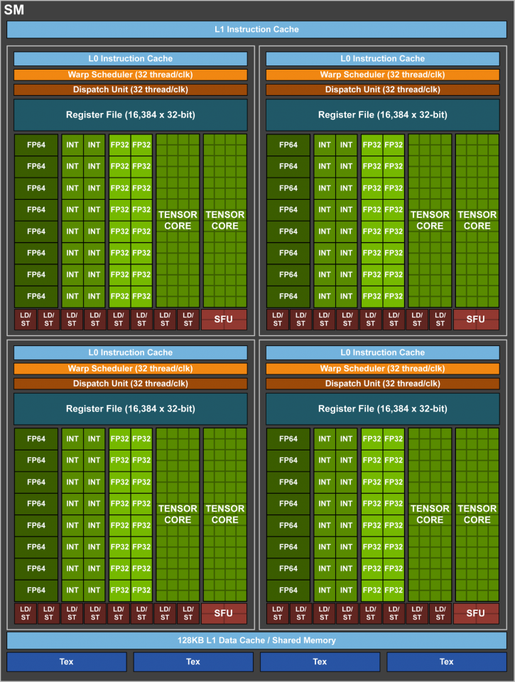
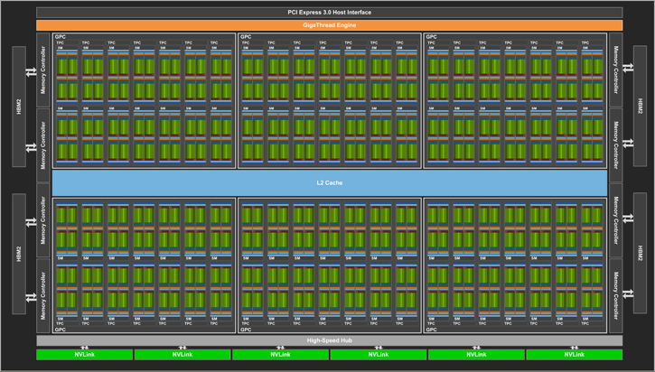
Slightly more detail first as there was some confusion with the Teslta Volta V100 specs and the GV100 GPU used, a fully enabled GV100 GPU actually consists of six GPCs, 84 Volta SMs, 42 TPCs (each including two SMs), and eight 512-bit memory controllers (4096 bits total). Each SM has 64 FP32 Cores, 64 INT32 Cores, 32 FP64 Cores, and 8 new Tensor Cores. Each SM also includes four texture units. 


With 84 SMs, a full GV100 GPU thus has a total of 5376 FP32 cores, 5376 INT32 cores, 2688 FP64 cores, 672 Tensor Cores, and 336 texture units. Each memory controller is attached to 768 KB of L2 cache, and each HBM2 DRAM stack is controlled by a pair of memory controllers. The full GV100 GPU includes a total of 6144 KB of L2 cache. The figure in above table shows a full GV100 GPU with 84 SMs (different products can use different configurations of GV100). The Tesla V100 accelerator uses 80 SMs. 

A new combined L1 data cache and shared memory subsystem of the Volta SM significantly improves performance while also simplifying programming and reducing the tuning required to attain at or near-peak application performance. Combining data cache and shared memory functionality into a single memory block provides the best overall performance for both types of memory accesses. The combined capacity is 128 KB/SM, more than 7 times larger than the GP100 data cache, and all of it is usable as a cache by programs that do not use shared memory. Texture units also use the cache. For example, if shared memory is configured to 64 KB, texture and load/store operations can use the remaining 64 KB of L1.


The  Tesla Volta V100 graphics processor

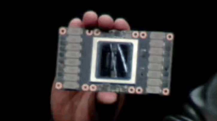
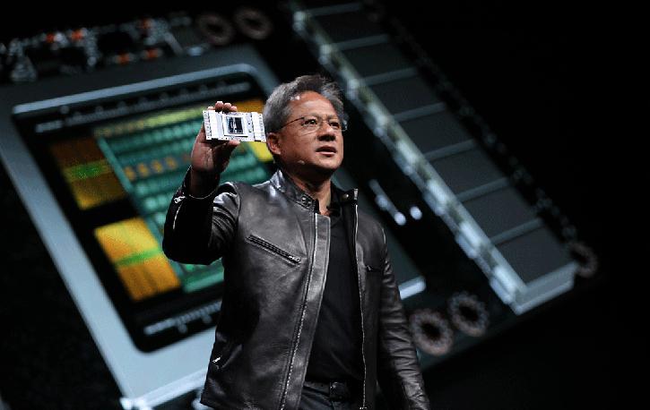
The Tesla Volta V100 graphics processor has 5,120 shader processors active and is based upon an incredible 21 Billion transistors. It offers what Nvidia calls 120 Tensor TeraFLOPS of performance. Gaming wise it would perform in the 15 TFLOP (fp32) region, delivered by a new type of architecture called Tensor cores. The R&D behind this did cost Nvidia many years and about $3 billion worth in investments, CEO JHH stated in his keynote. The first server and deep learning segmented products based on Tesla Volta V100 will become available in Q3 2017. The new Tensor Core is based on a 4×4 matrix array and fully optimized for deep learning. Nvidia stated, they felt Pascal is fast, but isn't fast enough. I already stated that the GPU is huge, it's 815mm2 huge and would fit roughly the palm of your hand.

  • Massive 815mm2 die size
  • 12nm FinFet (TSMC)
  • 21B Transistors
  • 15 FP32 TFLOPS / 7.5 FP64 TFLOPS
  • 120 Tensor TFLOPS
  • 16GB HBM2 which manages @ 900 GB/s
  • 5120 Shader processor cores

Tesla Volta V100 is capable of pushing 15 FP32 TFLOPS and much like Pascal GP100 is once again tied towards 4096-bit HBM2 graphics memory (stacked on-die cache). The unit will get 16GB of it divided over four stacks (= 4GB per stack). The memory is fabbed by Samsung. Volta’s 16GB HBM2 memory subsystem delivers 900 GB/sec peak memory bandwidth. This is 1.5x delivered memory bandwidth versus Pascal GP100. Tesla V100 delivers industry-leading floating-point and integer performance. Peak computation rates (based on GPU Boost clock rate) are:

  • 7.5 TFLOP/s of double precision floating-point (FP64) performance;
  • 15 TFLOP/s of single precision (FP32) performance;
  • 120 Tensor TFLOP/s of mixed-precision matrix-multiply-and-accumulate.

That HUGE die at 815 mm2 is fabbed by TSMC on a 12nm FFN fabrication process. In Q3 you will see the first enterprise based products based on Volta that start at 69.000 dollar. For us gamers, when GeForce GTX 1180 or 2080 will be released. That remains to be topic of a long discussion. Below a comparative specification list of the primary Tesla GPUs running up-to Volta, which runs in the 5120 shader processors at the 1.45 GHz marker for Boost frequency btw. It'll have 320 Texture Units, sheesh.


Click to enlarge

Tesla ProductTesla K40Tesla M40Tesla P100Tesla V100
GPU GK110 (Kepler) GM200 (Maxwell) GP100 (Pascal) GV100 (Volta)
SMs 15 24 56 80
TPCs 15 24 28 40
FP32 Cores / SM 192 128 64 64
FP32 Cores / GPU 2880 3072 3584 5120
FP64 Cores / SM 64 4 32 32
FP64 Cores / GPU 960 96 1792 2560
Tensor Cores / SM n/a n/a n/a 8
Tensor Cores / GPU n/a n/a n/a 640
GPU Boost Clock 810/875 MHz 1114 MHz 1480 MHz 1455 MHz
Peak FP32 TFLOP/s 5.04 6.8 10.6 15
Peak FP64 TFLOP/s 1.68 2.1 5.3 7.5
Peak Tensor Core TFLOP/s n/a n/a n/a 120
Texture Units 240 192 224 320
Memory Interface 384-bit GDDR5 384-bit GDDR5 4096-bit HBM2 4096-bit HBM2
Memory Size Up to 12 GB Up to 24 GB 16 GB 16 GB
L2 Cache Size 1536 KB 3072 KB 4096 KB 6144 KB
Shared Memory Size / SM 16 KB/32 KB/48 KB 96 KB 64 KB Configurable up to 96 KB
Register File Size / SM 256 KB 256 KB 256 KB 256KB
Register File Size / GPU 3840 KB 6144 KB 14336 KB 20480 KB
TDP 235 Watts 250 Watts 300 Watts 300 Watts
Transistors 7.1 billion 8 billion 15.3 billion 21.1 billion
GPU Die Size 551 mm² 601 mm² 610 mm² 815 mm²
Manufacturing Process 28 nm 28 nm 16 nm FinFET+ 12 nm FFN


Related Articles

Nvidia Turing GeForce 2080 (Ti) architecture review
It is almost time before we can present you our full review of the GeForce RTX series graphics cards. But first we'll be taking an architectural deep dive into the Turing graphics processors, and o...

Nvidia Testla Volta V100 and GV100 Preview
Nvidia announced the Testla Volta V100 processor, this is a Volta based GPU based on Tensor architecture. Tesla Volta V100 will be fabricated on a TSMC 12nm finfet process, pushing the limits of photo lithography as this GPU is huge.

Nvidia Titan X (Pascal) Extended Overclock Guide
Today an article slash guide dedicated on overclocking the Nvidia Titan X (Pascal). Are we able to pass 2000 MHz with the 12 Billion transistors based GPU ? Yes we can, realatively easily even. Armed ...

Nvidia Titan X (Pascal) Review
In this article we'll look at something that rises like Phoenix, the new generation Nvidia Titan X based on that all new Pascal GPU. Armed with 12GB of GDDR5X graphics memory and that all new GP102 G...

© 2023