Product PCB and component analysis
Product PCB and component analysis
Right, it's time get down to the nitty gritty - let's strip her nekked and see what is going on at the PCB components wise.

The cooling solution is fairly normal slash plain looking, it uses three thick heat-pipes that pass through a heatsink, with thermal paste tied to the all-copper block. Heatpipes wise, we've seen better really as three at 6mm is not a lot.
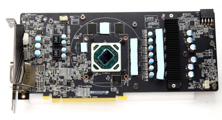
A fairly clean PCB. To the middle left the VRM area, in the middle, you can spot the Polaris GPU and surround it, the GDDR5 memory ICs. All critical components have been thermally padded including the VRM area chokes, MOSFET padding, and dedicated heatsink as well as DRAM memory chips padding. And everything padded is in touch with the cooler heatsink.
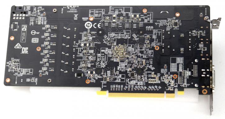
And the backside with the backplate removed. Let's run through some of the components though Mind you that the PCB and component usage for both the RX570 and RX580 MECH2 are identical, aside from the GPU that is.
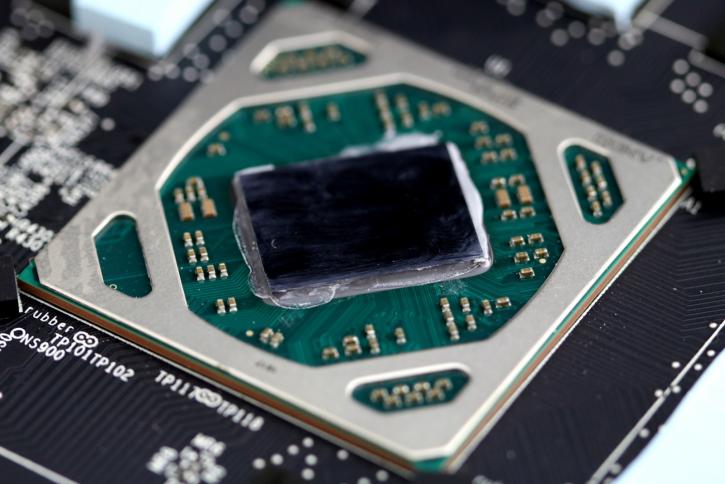
Okay, should we just call her Polaris or stick to Ellesmere? The Radeon RX 580 uses Polaris 20, also referred (read rebadged) by AMD as Ellesmere. The chip does not have an inscription on the die.
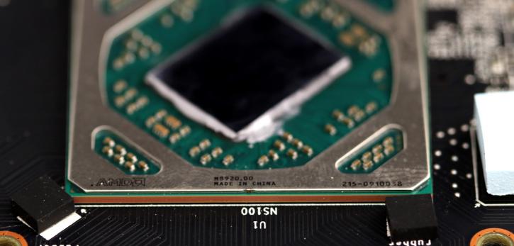
However, on the lower side, we can read out some data. The GPU is the same towards the original Polaris used on the RX 480, however, a newer FinFET+ fabrication process has been applied, offering better yields. The GPU has a die size of 232 mm². MSI applies thermal paste in-between the die and cooler surface area.
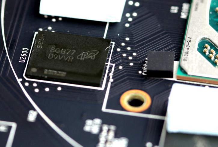
The memory then, MSI is making use of GDDR5 chips from Micron, it's a really familiar series, SKU code D9VVR is rated at 2000 MHz (=8000 MHz GDDR5 effective data-rate). You'll quite easily get 9 Gbps out of them really. We'll demonstrate that in the overclocking segment of this article. Both the RX570 and RX580 make use of this memory.
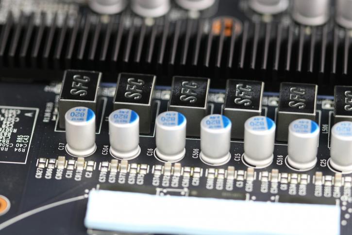
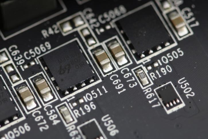
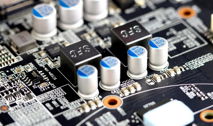
You can count them, MSI is listing the cards at 8 phases, which is correct. However, there are six phases for the GPU and then there are two more for memory. You can see solid core chokes (SFC), that would be molded inductor chokes (decreasing buzzing noises). Thej MOSFETs are covered with a heatsink, we'll look at them in a second.
So here the two additional phases organized as a 6+2 phase design. Across the PCB you see a clean component layout which includes VRM components.
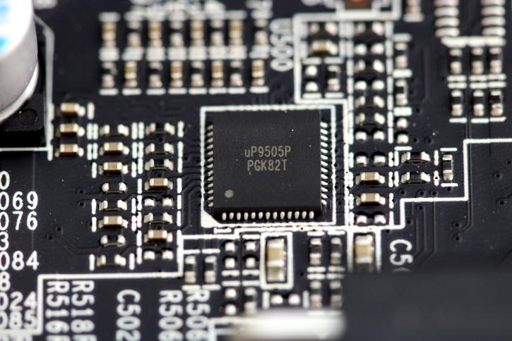
MSI upgraded its voltage regulator towards a newer chip from uPI Semiconductor - the uP9505P. From the top of my head, this phase buck controller can handle 6-phases.
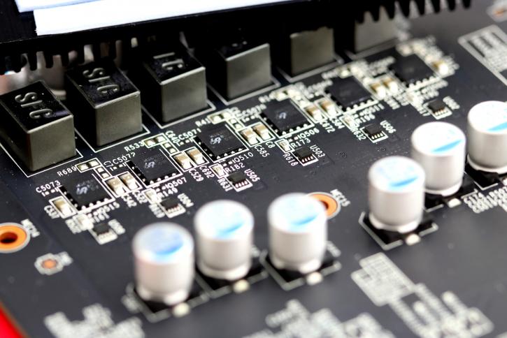
The rest is kept simple enough, we removed the MOSFET heatsink and it shows for each phase. The square chips to the left of the capacitors are MOSFETs.