Product Teardown
Teardown
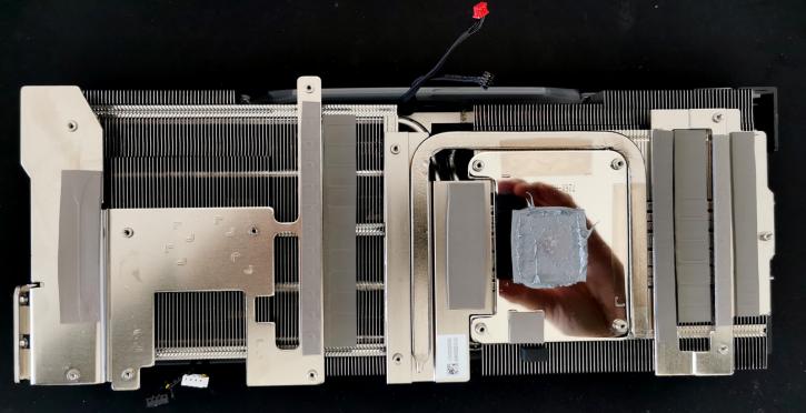
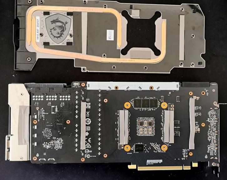
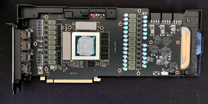
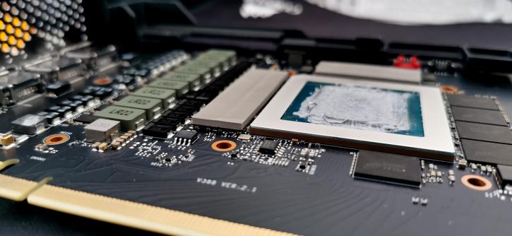
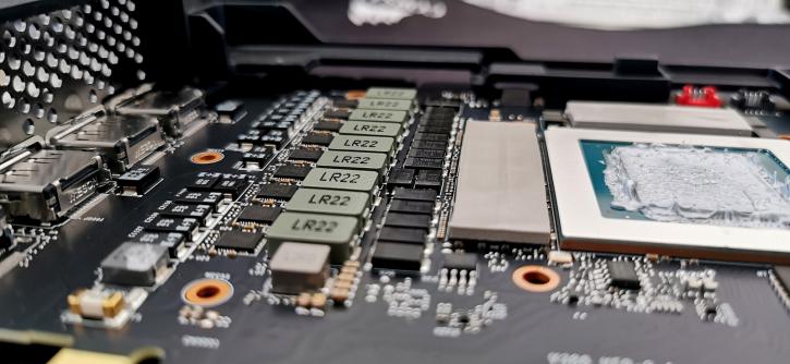
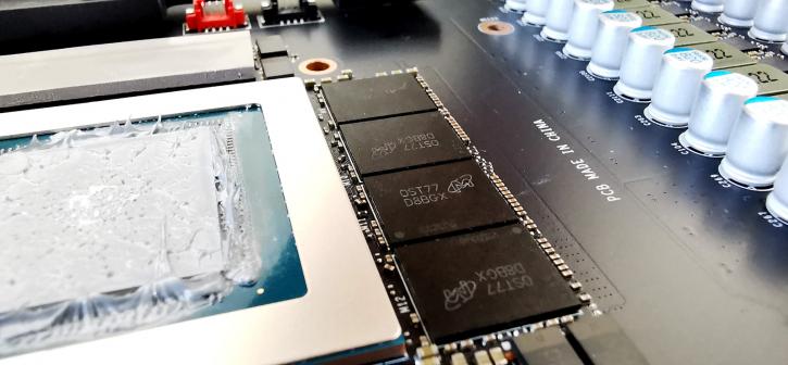
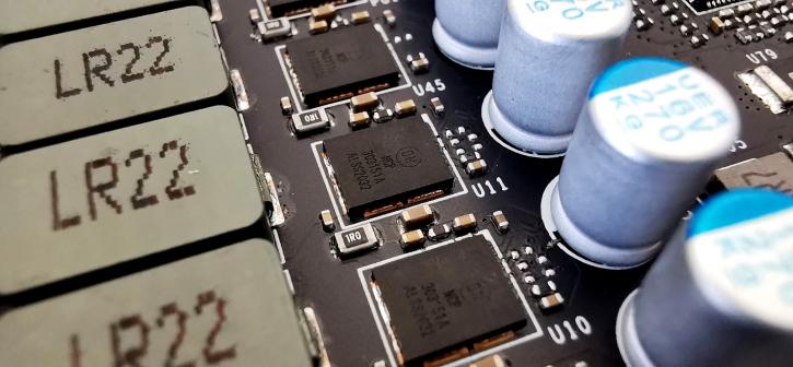
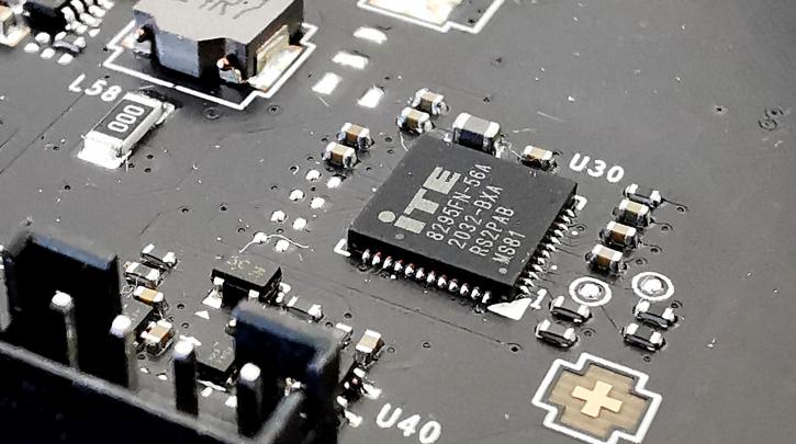
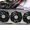
It is a request that is getting more and more daunting as we do not want to damage products. But user request on this is clear, you like a teardown and want to look to see what is going on at the PCB level. So here we go, meet the GA102-300 GPU, GPU and memory power phases, and GDDR6X memory from Micron labeled D8BGX, these are different from the ones used in the RTX 3080 labeled D8BGW. Looking at the PCB, what a gorgeous clean PCB/component design, look at that. 17 phased for GPU, four for memory. Of course, the board does need to be hooked up towards 3x 8-pin connectors, add 75W for PCIe and the board design is capable of delivering 525 Watt. You can see the LED system now integrated onto the PCB. So no more clumsy LED systems on the cooler side. All components are nicely cushioned with padding and heatsinks, most of them leading to the cooler.
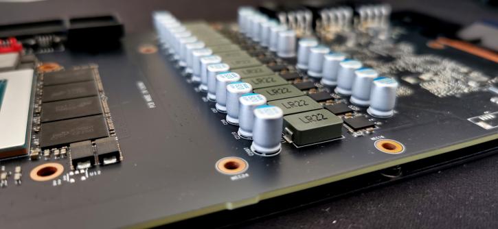
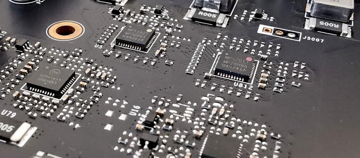
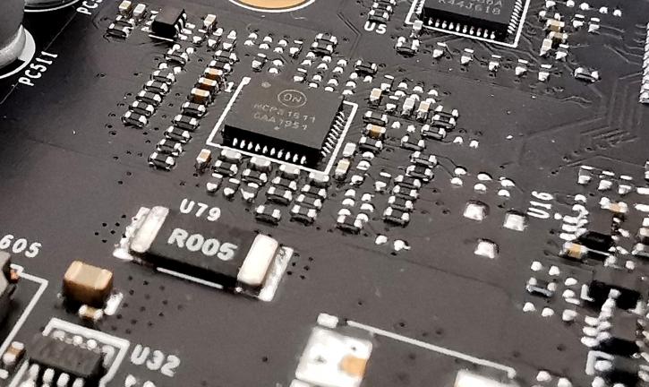
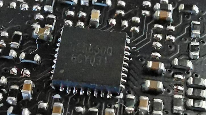
GPU voltage is fed by a 17-phase VRM backed by OnSemi NCP303151A DrMOS, managed by two brands UPI and OnSemi. There are four memory phases managed by UPI uS5650Q. Very noteworthy, the backplate is not just beautifully brushed aluminum, it has heat pipes that connect to the PCB and components, and actively helps with cooling. So that backplate cools actively.