
The Turing GPU
The Turing GPU
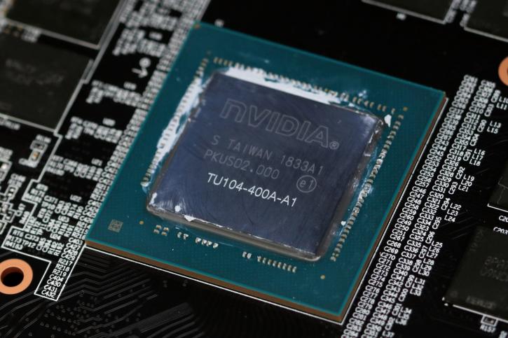
Looking at the Turing GPU, there is a lot of stuff you can recognize, but there certainly have been fundamental block changes in the architecture compared to say Pascal, the SM (Streaming Multiprocessor) clusters have separated, and now are core separated isolated blocks, something the Volta GPU architecture also shows as familiarity. Bear in mind that the base building block for all Turing GPUs will be the TU102, that is the flagship GPU that will be used on the GeForce RTX 2080 Ti. The GTX RTX 2080 will be using the chip called TU104. So the TU104 is a more simplified revision chip of the TU102, but shares the very same architecture.
Turing TU104 GPU Specifications
The TU104 counts 13.6 billion transistors localized onto a 545mm2 die. In comparison, Pascal had close to 12 billion transistors on a die size of 471mm2. Gamers will immediately look at the shader processors, it has 46 SMs (streaming multiprocessors) each holding 64 cores = 2944 Shader processors. It has 368 Tensor cores, 46 RT cores and 64 ROP units tied towards a total of 8GB GDDR6 graphics memory. This GPU is fabbed on an optimized 12nm TSMC FinFET+ node. We've placed the main specifications in a table overview.
|
| ||||||
|---|---|---|---|---|---|---|
| GeForce | RTX 2080 Ti FE | RTX 2080 Ti | RTX 2080 FE | RTX 2080 | RTX 2070 FE | RTX 2070 |
| GPU | TU102 | TU102 | TU104 | TU104 | TU106 | TU106 |
| Node | TSMC 12 nm FFN | |||||
| Die Size mm² | 754 | 545 | 445 | |||
| Shader cores | 4352 | 4352 | 2944 | 2944 | 2304 | 2304 |
| Transistor count | 18.6 Billion | 18.6 Billion | 13.6 Billion | 13.6 Billion | 10.8 Billion | 10.8 Billion |
| Base frequency | 1350 MHz | 1350 MHz | 1515 MHz | 1515 MHz | 1410 MHz | 1410 MHz |
| Boost frequency | 1635 MHz | 1545 MHz | 1800 MHz | 1710 MHz | 1710 MHz | 1620 MHz |
| Memory | 11GB GDDR6 | 11GB GDDR6 | 8GB GDDR6 | 8GB GDDR6 | 8GB GDDR6 | 8GB GDDR6 |
| Memory frequency | 14 Gbps | 14 Gbps | 14 Gbps | 14 Gbps | 14 Gbps | 14 Gbps |
| Memory bus | 352-bit | 352-bit | 256-bit | 256-bit | 256-bit | 256-bit |
| Memory bandwidth | 616 GB/s | 616 GB/s | 448 GB/s | 448 GB/s | 448 GB/s | 448 GB/s |
| L2 Cache | 5632 KB | 5632 KB | 4096 KB | 4096 KB | 4096 KB | 4096 KB |
| RT cores | 68 | 68 | 46 | 46 | 36 | 36 |
| Tensor cores | 544 | 544 | 368 | 368 | 288 | 288 |
| Texture units | 272 | 272 | 184 | 184 | 144 | 144 |
| ROPs | 96 | 96 | 64 | 64 | 64 | 64 |
| TDP | 260W | 250W | 225W | 215W | 185W | 175W |
| Power connector | 2x 8-pin | 2x 8-pin | 8+6-pin | 8+6-pin | 8-pin | 8-pin |
| NVLink | Yes | Yes | Yes | Yes | - | - |
| Performance (RTX Ops) | 78T RTX-Ops | 60T RTX-Ops | 45T RTX-Ops | |||
| Performance (RT) | 10 Gigarays/s | 8 Gigarays/s | 6 Gigarays/s | |||
| TFlops fp32 | 14.2 / 13.4 | 10.6 / 10 | 7.9 / 7.5 | |||
| Max Therm degree C | 89 | 89 | 89 | |||
| price | $ 1199 | $ 999 | $ 799 | $ 699 | $ 599 | $ 499 |
Turing architecture
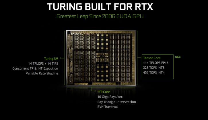
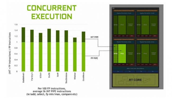
We'll try and be brief here, but Turing is a new and completely overhauled architecture that actually has gotten a new SM (Streaming Multiprocessor) design. As I mentioned, it has a bit of everything, but mostly it hints towards Volta. Two SMs are included per TPC (Texture / Processor Cluster - a group made up of several SMs). Each SM has a total of 64 FP32 Cores and 64 INT32 Cores. Now before you get all confused, yes, that is radically different from Pascal (GeForce series 1000) which had one SM per TPC and 128 FP32 Cores per SM. The Turing SM architecture supports parallel execution of FP32 and INT32 operations, independent thread scheduling similar to the Volta GV100 GPU. That's also described as concurrent execution of FP32 and INT32 operation. Each Turing SM holds eight Turing Tensor Cores. With that out of the way, have a peek at the block diagram below.
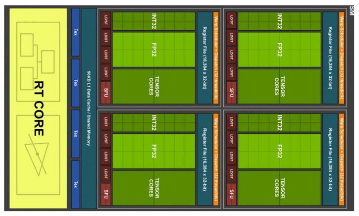
Each Turing SM is partitioned into four processing blocks, each holds 16 FP32 Cores, 16 INT32 Cores, two Tensor Cores, one warp scheduler, and one dispatch unit. Each block includes a new L0 instruction cache and a 64 KB register file. The four processing blocks share a combined 96 KB L1 data cache/shared memory. Traditional graphics workloads partition the 96 KB L1/shared memory as 64 KB of dedicated graphics shader RAM and 32 KB for texture cache and register file spill area. Compute workloads can divide the 96 KB into 32 KB shared memory and 64 KB L1 cache, or 64 KB shared memory and 32 KB L1 cache.
Concurrent Execution of Floating Point (fp32) and Integer Instructions (int32)
Turing’s SM initiates a new unified architecture for shared memory, L1, and texture caching. This unified design allows the L1 cache to leverage resources, increasing its bandwidth by 2x per TPC compared to Pascal, and allows it to be reconfigured to grow larger when shared memory allocations are not using all the shared memory capacity. The Turing L1 can be as large as 64 KB in size, combined with a 32 KB per SM shared memory allocation, or it can reduce to 32 KB, allowing 64 KB of allocation to be used for shared memory. Turing’s L2 cache capacity has also been increased. Combining the L1 data cache with the shared memory reduces latency and provides higher bandwidth than the L1 cache implementation used previously in Pascal GPUs. NVIDIA claims these changes in SM enable Turing to achieve 50% improvement in delivered performance per CUDA core.
Caches and ROPs
Turing GPUs add larger and faster L2 caches in addition to the new GDDR6 memory subsystem. The TU102 GPU and it's derivatives ships with 6 MB of L2 cache, double the 3 MB of L2 cache that was offered in the prior generation GP102 GPU used in the TITAN XP. TU102 also provides significantly higher L2 cache bandwidth than GP102. Like prior generation NVIDIA GPUs, each ROP partition in Turing contains eight ROP units and each unit can process a single-color sample. A full TU102 chip contains 12 ROP partitions for a total of 96 ROPs.
Graphics memory - GDDR6
Allow me to quickly inject a paragraph here. Another difference in-between Volta and Turing is graphics memory. HBM2 is a bust for consumer products, at least it seems and feels that way. The graphics industry at this time is clearly favoring the new GDDR6. It’s easier and cheaper to fab and add and at this time can even exceed HBM2 in performance. The previous GeForce GTX 1080 with the latest GDDR5X memory could run 11 Gbps, often tweakable towards the 12 Gbps range. GDDR6 graphics memory will be faster and more energy efficient. The memory is advancing on GDDR5X (Graphics Double Data Rate (DDR)) but with a memory bandwidth of 14 Gbit/s it offers almost twice as much as GDDR5 (not GDDR5X) offers. In the near future, GDDR6 could transfer data at 16Gbps (bits per second), which is twice as fast as regular GDDR5. The GeForce RTX 2070 (8GB 256-bit), 2080 (8GB 256-bit) and 2080 Ti (11GB 352-bit) series will be paired with 14 Gbps GDDR6.
