Reference technology and specs
Reference technology and specs
In this segment of the article we will look at the reference (original design) based specs and architecture. The GeForce GTX 660 is based on the Kepler GPU architecture. The product however is using a new chip called the GK106 which is based on a 28nm fabrication process. The chip has a transistor count of 2.54 Billion for those that care.
- The GeForce GTX 660 boasts 960 CUDA (shader) cores
- The GeForce GTX 660 Ti boasts 1344 CUDA (shader) cores
- The GeForce GTX 670 boasts 1344 CUDA (shader) cores
- The GeForce GTX 680 boasts 1536 CUDA (shader) cores
And yeah that says it all right there, that's the same amount of shader cores and thus rendering engine compared to the GTX 670. It is 576 Shader cores less then 1536 and precisely three CUDA core cluster (SM) less out of the eight available on a GK104 chip.
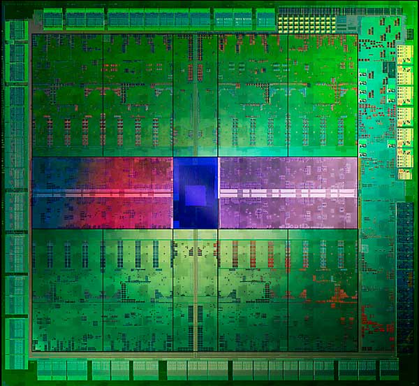 NVIDIA GK104 Kepler architecture GPU, you can see the eight SM (CUDA/shader core) clusters, (NVIDIA has not provided a GK106 die shot).
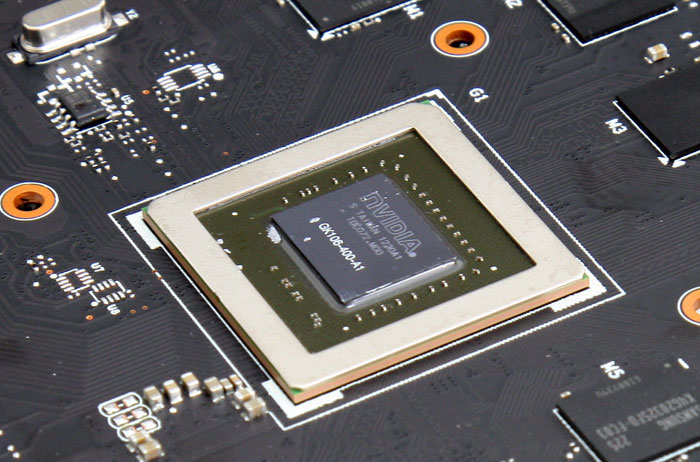
A photo of the NVIDIA GK106 Kepler architecture based GPU
Five SM (shader) clusters each have 192 shader processors. Five is a bit of an unusual number on the world of mathematics you want even numbers really. So really expect eh GK106 to have six SM clusters. NVIDIA has not provided us a die shot to confirm our theory.
Anyway, the GPU core versus the shader processor domain are both clocked 1:1, meaning both the core and shader domain clock in at 980 MHz. The boost clock for the reference GTX 660 cards is set at 1033 MHz though that can vary a bit per card and available power envelope.
192-bit Memory Interface
Like certain prior GeForce GPUs, the GeForce GTX 660s memory controller supports mixed density memory module operation. This feature allows us to outfit the board with 2GB of memory (instead of 1.5GB) while utilizing a 192-bit memory interface. The memory controller logic divides the GTX 660s eight memory modules as follows:
- Memory Controller 1: 4 pcs: 128M x 16 GDDR5 (1GB, 16-bit mode)
- Memory Controller 2: 2 pcs: 64M x 32 GDDR5 (512MB, 32-bit mode)
- Memory Controller 3: 2 pcs: 64M x 32 GDDR5 (512MB, 32-bit mode)
The three memory controllers segment the memory into equal size fragments of 512MB each to create a frame buffer size of 1.5GB and 192-bit interface. The remaining 512MB of memory is accessed in an additional memory transaction by memory controller 1 with a 64-bit width. This gives the GPU access to a full 2GB of video memory with minimal latency.
So 192-bit memory bus is being used, but it remains clocked at an affective data rate of 6 Gbps. On the memory controller side of things you'll see very significant improvements as the reference memory clock is set at 6 GHz / Gbps.
This boils down to to a memory bandwidth of 192 GB/s on the 256-bit memory bus for the GTX 670 and 680 but roughly 144 GB/s for the GTX 660 and Ti (which is still very sufficient). The product is obviously PCI-Express 3.0 ready and has a TDP of around 140 Watt.
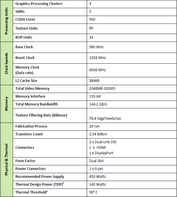
We already mentioned it, another change is the ROP (raster operation) engine, cut down to 24 units opposed to 32 on it's bigger brothers. With this release, NVIDIA now has the real mid-range products on its way. The new graphics adapters are of course DirectX 11.1 ready.
With Windows 8, 7 and Vista also being DX11 ready all we need are more new games to take advantage of DirectCompute, multi-threading, hardware tessellation and the latest shader 5.0 extensions. For your reference here's a quick overview of some of the more recent graphics cards.
| GeForce GTX 580 |
GeForce GTX 660 |
GeForce GTX 660 Ti |
GeForce GTX 670 |
GeForce GTX 680 |
GeForce GTX 690 | |
| Stream (Shader) Processors | 512 | 960 | 1344 | 1344 | 1536 | 3072 |
| Core Clock (MHz) | 772 | 980 | 915 | 915 | 1006 | 915 |
| Shader Clock (MHz) | 1544 | - | - | - | - | - |
| Boost clock (Mhz) | - | 1033 | 980 | 980 | 1058 | 1019 |
| Memory Clock (effective MHz) | 4000 | 6008 | 6008 | 6008 | 6008 | 6008 |
| Memory amount | 1536 | 2048 | 2048 | 2048 | 2048 | 4096 |
| Memory Interface | 384-bit | 192-bit | 192-bit | 256-bit | 256-bit | 256-bit |
| Memory Type | GDDR5 | GDDR5 | GDDR5 | GDDR5 | GDDR5 | GDDR5 |
For Kepler, NVIDIA kept their memory controllers GDDR5 compatible. Memory wise NVIDIA has nice large memory volumes due to their architecture, we pass 2 GB as standard these days for most of NVIDIA's series 600 graphics cards in the high range spectrum.
