SMT process
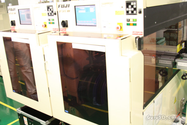
Check out the loader of this unit by the way. And let me try and take a photo through that glass...
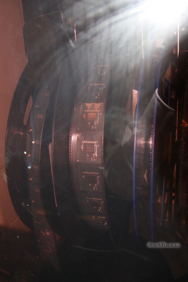
Yeah the photo had to be big for you to understand and grasp what is going on inside there. These big rolls have (in this build) the Intel chipset as in North- and Southbridge chips. Looks like P45 if I'm not mistaken.
After all components are mounted the PCB will pass through a Heller 1900EXL hot convection oven. Here is where the solder paste fully melts and sets, securing the components in position. Baked like chocolate chipped cookies.
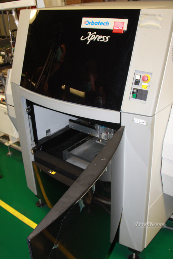
Once the last SMD components are soldered they pass through this machine, and luckily they opened it up for us. This is an optical tester. And within seconds it will have automatically tested the processed PCB board for missing or improperly installed components.
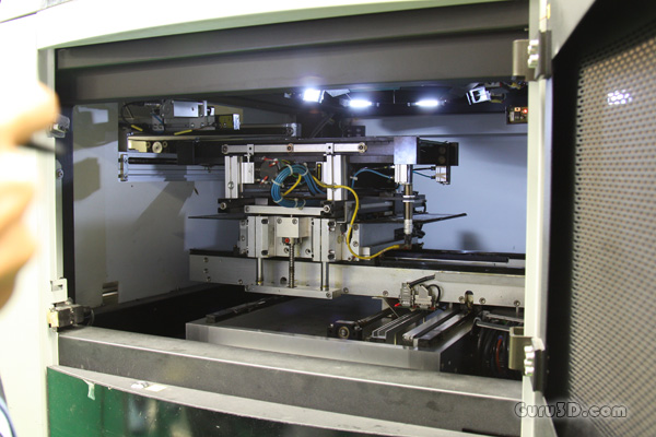
Here's the inside of that machine. Next time I'll bring a video camera and show you a video, as that is massively impressive.
