GeForce GTX 480 Specifications
GeForce GTX 480 Specifications
Alright, let's get this article started, as always we'll have a look at Geforce GTX 480 reference (and 470 as well) specifications first.
NVIDIA released two high-end class DirectX 11 capable products. First off, the graphics adapters are of course DirectX 11 ready. With Windows 7 and Vista also being DX11 ready all we need are some games to take advantage of DirectCompute, multi-threading, Hardware Tessellation and new shader 5.0 extensions. DX11 is going to be good and once tessellation kicks into games, much better looking.
These are the bold numbers:
- GeForce GTX 480 : 480 SP, 384-bit, 250W TDP, US$ 449~499
- GeForce GTX 470 : 448 SP, 320-bit, 225W TDP, US$ 299~349
- GeForce GTX 465 : 352 SP, 256-bit, 200W TDP, US$ 279~289
Some of you will say "huh?" as everybody expected 512 shader processors on the top of the line model, 272 cores more than the GT200 (GeForce GTX 280/285). We were as much surprised as you guys when we learned that it turned out to be 480 shader processors for the GeForce GTX 480. See, the Fermi architecture, the GF100 graphics processor has sixteen shader clusters embedded in it (called SMs). For the GeForce GTX 480 one such a cluster is disabled, and on the GeForce GTX 470 (though expected) two are disabled.
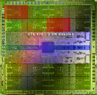
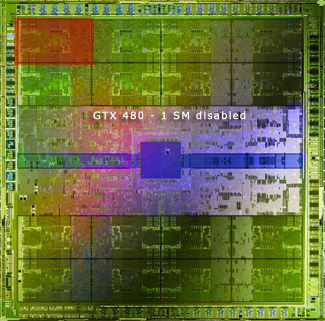
As to why one SM is disabled on the GeForce GTX 480, we can only speculate. But we have reason to believe that NVIDIA did this to secure better yields and ramp volume production up. Also, much like the GeForce GTX 260 SP216, for the future to be able to introduce a slightly faster SKU with the full 512 SPs. The reality remains that it will not matter 'heaps' in terms of performance as you lose only one-sixteenth of shader performance.
The GeForce GTX 400 cards have the Fermi family chip embedded on them. That chip is called GF100. The GF100 GPU is placed onto an 8-layer PCB and tied to gDDR5 memory. On the topic of graphics memory; NVIDIA made their memory controller GDDR5 compatible, which was not the case on GT200 based GeForce GTX 260/275/285/295, hence their GDDR3 memory.
Memory wise expect large, exemplary large numbers, as we are passing 1 GB. Each utilized memory controller on the respective GPU will get 256MB of memory tied to it.
- The GTX 470 has five memory controllers (5x256MB) = 1280 MB of GDDR5 memory
- The GTX 480 has six memory controllers (6x256MB) = 1536 MB of GDDR5 memory
As you can understand, the massive memory partitions, bus-width and combination of GDDR5 memory (quad data rate) allows the GPU to work with a very high framebuffer bandwidth. So we had a chat about the GF100 GPU and memory. It's now time to break down the GPU clocks:
| GeForce 9800 GTX |
GeForce GTX 285 |
GeForce GTX 295 |
GeForce GTX 470 |
GeForce GTX 480 | |
| Stream (Shader) Processors | 128 | 240 | 240 x2 | 448 | 480 |
| Core Clock (MHz) | 675 | 648 | 576 | 607 | 700 |
| Shader Clock (MHz) | 1675 | 1476 | 1242 | 1215 | 1400 |
| Memory Clock (effective MHz) | 2200 | 2400 | 2000 | 3350 | 3700 |
| Memory amount | 512 MB | 1024 MB | 1792 MB | 1280 | 1536 |
| Memory Interface | 256-bit | 512-bit | 448-bit x2 | 320-bit | 384-bit |
| Memory Type | gDDR2 | gDDR3 | gDDR3 | gDDR5 | gDDR5 |
| HDCP | Yes | Yes | Yes | Yes | Yes |
| Two Dual link DVI | Yes | Yes | Yes | Yes | Yes |
| HDMI | No | No | No | Yes | Yes |
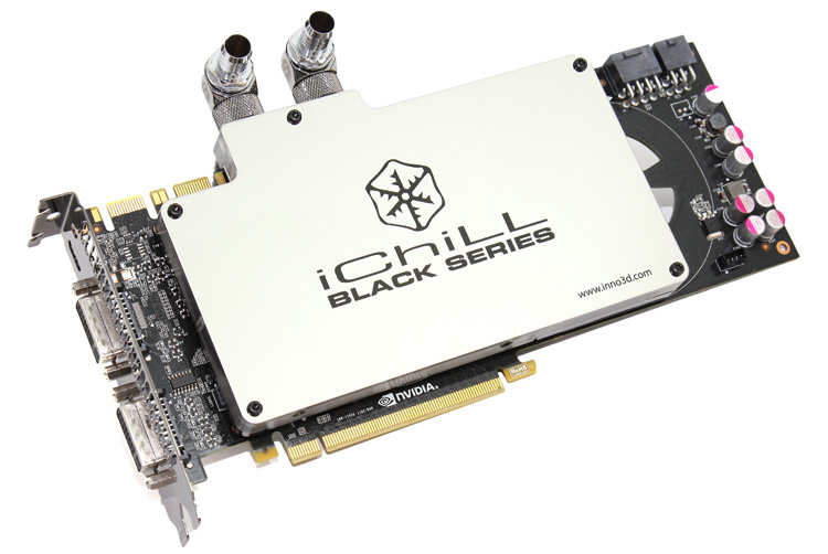
Inno3D altered a thing or two though ...