
What's SATA | NAND Types
So what is NVMe?
NVMe (non-volatile memory express) is a host controller interface and storage protocol created to accelerate solid-state drive (SSD) transfer over a computer's high-speed Peripheral Component Interconnect Express (PCIe) bus.
NVMe-based PCIe SSDs over SATA-based ones include reduced latency in the host software stack, higher input/output operations per second (IOPS), and potentially lower power consumption, depending on the form factor and the number of PCIe lanes in use.
Moving from PCIe Gen 2 to Gen 3 doubles the bandwidth available to install add-on cards, from 500 MB/s per lane to 1 GB/s per lane. A Gen 3.0 PCI Express x16 slot can offer 16 GB/s of bandwidth in each direction. That gives us a bi-directional bandwidth of up to 32 GB/s in total. PCIe 4.0 once again doubles that up. Obviously, the hardware you use needs to be Gen 4.0 compatible.
Below, you can see a breakdown of PCI-Express bandwidth per lane in the individual revisions:
- PCI-Express 1.1 sends 250 MB/s in each direction
- PCI-Express 2.0 sends 500 MB/s in each direction
- PCI-Express 3.0 sends 1 GB/s in each direction
- PCI-Express 4.0 sends 2 GB/s in each direction
NVMe M.2 units need to be able to use whatever is assigned to them, which is why most modern motherboards and drives are compatible with an x4 link, so if you have a Gen 4.0 x4 link, it can handle a total bandwidth of 16 GB/s (bi-directional) in PCIe Gen 4.0 mode. In contrast, an old Gen 1.0 x16 slot could only be 2 GB/ s (bi-directional). This bandwidth, combined with fast NAND and a top-notch controller, allows for massive storage speeds.
SATA (including SATA 3/6Gbps) Explained
SATA I (revision 1. x), formally known as SATA 1.5Gb/s, is the first generation of the SATA interface, running at 1.5 Gb/s, and it supports a bandwidth of up to 150MB/s. SATA II (revision 2. x), formally known as SATA 3Gb/s, is the second generation of the SATA interface, running at 3.0 Gb/s, and it supports a bandwidth of up to 300MB/s.
SATA III (revision 3. x), formally known as SATA 6Gb/s, is the third generation of the SATA interface, running at 6.0 Gb/s. It supports a bandwidth of up to 600MB/s (due to the overhead, tolerances, error correction, and random occurrences, it's not the theoretical 750 MB/s) and is backward compatible with the SATA 3 Gb/s interface.
What Is NAND?
NAND flash memory is a non-volatile storage technology that does not require power to retain data. Introduced by Toshiba in 1984, flash memory was developed from EEPROM (electrically erasable programmable read-only memory). An important goal of NAND flash development has been to reduce the cost per bit and increase maximum chip capacity so that flash memory can compete with magnetic storage devices, such as hard disks. NAND flash has found a market in devices where large files are frequently uploaded and replaced. MP3 players, digital cameras, and USB flash drives use NAND technology.
NAND Types
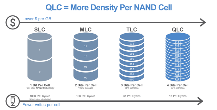
SLC
Single-level cell NAND stores a single bit per cell, offering the highest endurance of the three types. It takes up more die space per capacity, restricting the possible capacity options and increasing prices. SLC is limited to the enterprise area, where endurance is the most vital feature needed. SLC memory cells can withstand up to 100,000 write cycles before failing.
MLC
Multi-level cell NAND stores multiple bits per cell, but that name can be misleading. While technically, it could go beyond 2 bits per cell; it typically equates to just 2 bits per cell. It has a lower endurance than SLC but is better than TLC. A 2-bit MLC memory cell can typically withstand up to 10,000 write cycles before failing. You will find this in most enthusiast drives, which deliver a tremendous read-and-write performance.
TLC
Triple-level cell NAND is the latest addition to the range, and it also stores multiple bits per cell, three to be exact. TLC has the lowest endurance of the three types but offers the largest capacities for the smallest prices. Manufacturers have improved the endurance and reliability of TLC NAND a lot through a refined manufacturing process, error correction codes, and wear-leveling algorithms. A TLC memory cell can sustain about 1,000 write cycles before failing, which is why thus far, it has been limited to consumer-grade applications.
QLC
QLC NAND writes 4 bits per cell. QLC has a 33% higher storage density than TLC, and each cell can save 4-bit data. Besides, the write cycle of QLC could reach 1000 times, which is equal to or even better than TLC. At the same time, QLC costs less than TLC. The performance and life span of QLC are not as good as that of SLC or MLC and worse than TLC.
