
Maxwell GPU Architecture
Maxwell Graphics Architecture
Let's place the more important data on the GPU into a chart to get an idea and better overview of changes in terms of architecture like shaders, rops and where we are at frequencies wise:
| GeForce | GTX Titan X | GTX Titan Black | GTX 980 Ti | GTX 980 |
|---|---|---|---|---|
| GPU | GM200 | GK110B | GM200 | GM204 |
| Architecture | Maxwell | Kepler | Maxwell | Maxwell |
| Transistor count | 8 Billion | 7.1 Billion | 8 Billion | 5.2 Billion |
| Fabrication Node | TSMC 28 nm | TSMC 28 nm | TSMC 28 nm | TSMC 28 nm |
| CUDA Cores | 3072 | 2880 | 2816 | 2048 |
| SMMs / SMXs | 24 | 15 | 22 | 16 |
| ROPs | 96 | 48 | 96 | 64 |
| FP64 | 1/32 FP32 | 1/3 FP32 | 1/32 FP32 | 1/32 FP32 |
| GPU Clock Core / Boost | 1002 MHz / 1076 MHz | 889 MHz / 980 MHz | 1002 MHz / 1076 MHz | 1127 MHz / 1216 MHz |
| Memory Clock | 1753 MHz | 1753 MHz | 1753 MHz | 1753 MHz |
| Memory Size | 12 GB | 6 GB | 6 GB | 4 GB |
| Memory Bus | 384-bit | 384-bit | 384-bit | 256-bit |
| Memory Bandwidth | 337 GB/s | 337 GB/s | 337 GB/s | 224 GB/s |
| FP Performance | 7.0 TFLOPS | 5.20 TFLOPS | 6.4 TFLOPS | 4.61 TFLOPS |
| GPU Thermal Threshold | 91 Degrees C | 95 Degrees C | 91 Degrees C | 95 Degrees C |
| TDP | 250 Watt | 250 Watt | 250 Watt | 165 Watt |
| Launch MSRP | $999 | $999 | TBA | $549 |
So we talked about the core clocks, specifications and memory partitions. However, to be able to better understand a graphics processor you simply need to break it down into small pieces. Let's first look at the raw data that most of you can understand and grasp. This bit will be about the Maxwell GM200 architecture. NVIDIA’s “Maxwell” GPU architecture implements a number of architectural enhancements designed to extract even more performance and more power efficiency per watt consumed.
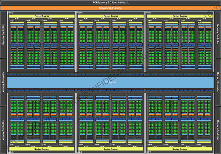
So above, we see the GM200 block diagram that entails the Maxwell architecture, Nvidia started developing the Maxwell architecture around 2011/2012 already. Each of the GPCs has eight SMX/SMM (streaming multi-processor) clusters in total. You'll spot six 64-bit memory interfaces, bringing in a 386-bit path to the graphics memory at 7 Gbps.
Let's break it down into bits and pieces. A fully enabled GM200 GPU will have (again fully enabled, the GTX 980 Ti for example is slightly cut down):
- 3072 CUDA/Shader/Stream processors
- There are 128 CUDA cores (shader processors) per cluster
- Over 8 Billion Transistors
- 256 Texture units
- 96 ROP units
- 3MB L2 cache
- 384-bit GDDR5

One SMX: 128 single‐precision shader cores, double‐precision units, special function units (SFU), and load/store units. So based on a full 24 SMM 3072 shader core chip the SMX looks fairly familiar in design. In the pipeline we run into the ROP (Raster Operation) engine and the GM200 has a nice 96 engines for features like pixel blending and AA. The GPU has 64 KB of L1 cache for each SMX plus a special 48 KB texture unit memory that can be utilized as a read-only cache. The GPU’s texture units are a valuable resource for compute programs with a need to sample or filter image data. The texture throughput is significantly decreased compared to Fermi – each SMX unit contains 8 texture filtering units.
- GeForce GTX 960 has 8 SMX x 8 Texture units = 64
- GeForce GTX 970 has 13 SMX x 8 Texture units = 104
- GeForce GTX 980 has 16 SMX x 8 Texture units = 128
- GeForce GTX 980 Ti has 22 SMX x 8 Texture units = 176
- GeForce GTX Titan X has 24 SMX x 8 Texture units = 192
So there's a total of up-to 22 SMX x 8 TU = 176 texture filtering units available for the silicon itself (once all SMXes are enabled).
Typically lower is worse, but these cards however require little voltage and can be clocked very high. And that's where performance kicks in at low power consumption. To reduce DRAM bandwidth demands, NVIDIA GPUs make use of lossless compression techniques as data is written out to memory. The bandwidth savings from this compression are realized a second time when clients such as the Texture Unit later read the data. As illustrated in the preceding figure, the compression engine has multiple layers of compression algorithms. Any block going out to memory will first be examined to see if 4x2 pixel regions within the block are constant, in which case the data will be compressed 8:1 (i.e., from 256B to 32B of data, for 32b color). If that fails, but 2x2 pixel regions are constant, they will compress the data 4:1. These modes are effective for AA surfaces, but less so for 1xAA rendering. Therefore, starting in Fermi Nvidia also implemented support for a “delta color compression” mode. In this mode, they calculate the difference between each pixel in the block and its neighbor, and then try to pack these different values together using the minimum number of bits. For example if pixel A’s red value is 253 (8 bits) and pixel B’s red value is 250 (also 8 bits), the difference is 3, which can be represented in only 2 bits. If the block cannot be compressed in any of these modes, then the GPU will write out data uncompressed, preserving the lossless rendering requirement. The effectiveness of delta color compression depends on the specifics of which pixel ordering is chosen for the delta color calculation. Maxwell contains the third generation of delta color compression, which improves effectiveness by offering more choices of delta calculation to the compressor. Thanks to the improvements in caching and compression in Maxwell, the GPU is able to significantly reduce the number of bytes that have to be fetched from memory per frame. Maxwell uses roughly 25% fewer bytes per frame compared to Kepler.
