2 - The GeForce GTX series 200 GPU
So then, let's face it .. the Radeon HD 4870 is a thorn in the green colored UV reflective eyes of NVIDIA as pricing wise this thing just does wicked things. To adapt to ATI's strategy, NVIDIA lowered their prices big-time and then introduced this new SKU. NVIDIA was seeking more performance in the GTX 260 series -- they needed to give it a little more bite. So NVIDIA unleashed its GeForce GTX 260 Core 216 and started working on their "Big Bang" drivers, which too me still sounds a little sexual. You can't imagine the fantasies I had when I noticed their "Big Bang II" drivers being "released".
The GeForce GTX series 200 GPUs
NVIDIA launched the GeForce GTX series 200. This launch included both the GeForce GTX 260 and 280, now in several flavors.
The new GTX series 200 GPUs are big man, with roughly 1400 million transistors. It's the biggest chip that NVIDIA has ever built, with 1400M transistors it's a freak on a leash. To compare to, the GeForce 8800 'only' had roughly 700 Million processors. So that's roughly doubling up the previous transistor count. Interestingly enough, that would also double up the die-size of the processor and so you'd expect NVIDIA to move to a smaller fabrication process for this graphics processor. They did not as the new architecture is still based on a 65nm fabrication size. The chip is being made at TSMC and the biggest one they've ever made.
It resulted in a huge die measuring 24 x 24 mm. And not many chips will actually fit on a 300 mm wafer, since , resulting in a die area size of 576 mm2. We'll show you a photo I took of that die area later on, but I measured and it's indeed easily 5.5 cm. I have no clue how a chip this big really yields, but this certainly is one expensive graphics processor to make. We do expect NVIDIA to move to a smaller fab process (55nm) later in Q4 2008.
Let's walk through some of the main features (you need to stamp into your head) of this new beast:
Obviously a big chunk of the transistors are being utilized for the shader cores. And shader cores the product surely has:
- 240 of them on the GeForce GTX 280.
- 216 cores on the GeForce GTX 260 Core 216
- 192 cores on the GeForce GTX 260
The new shader architecture has some cool new features. Sitting in-between them now is an integration of local cache memory (16k software managed cache). It is sitting in-between a block with 8 shader cores. So simply put, what helps here is that the data / instruction doesn't have to leave the GPU anymore to crunch it's data (normally done in the regular frame buffer memory). This is a significant improvement in the architecture. You already spotted it, the new GeForce GTX 260 Core 216 has 216 Shader Processors (SPs).
- Inside the GTX 200 series GPU, the shaders cores are clustered in three blocks of eight shader processors.
- Now we know that there are ten clusters totaling up towards the 240 shader units for the GeForce GTX 280.
So the GTX 280 has 10x3x8= 240 Shader Processors.
Therefore a standard GTX 260 has to have 8x3x8= 192 SPs.
Now with the info above that I just mentioned, you can do the math with me real quick. The regular GeForce GTX 260 has got to have 8 shader clusters and thus 192 shader processors which you can utilize for gaming ... or computing other stuff.
What does this mean, well:
- 3x8=24
- 24x9=216 cores.
The entire GTX 200 series is all one and the same chip. This new Core 216 GPU is in fact a full fetched GTX 280 core with one cluster laser-cut and deactivated. 1.4 Billion transistors .. really it's piece of art to look at. Check out the photo below.
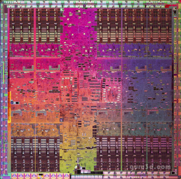
GeForce Series 280 architecture - Look closely and spot the 10 shader clusters. On the GTX 260 Core 216 one has been disabled.
