Page 4
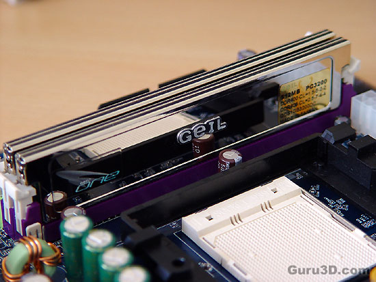
Right, GEIL memory. As you already noticed, this product is made for a rather specific category of PC users, tweakers and overclockers. People who tweak the crap out of their system, I like to call them enthusiasts or if you want, Guru3D's audience. To be able to test this product to it's fullest potential we will need to either tweak or overclock the PC and of course we'll do just that.
Understanding memory timings
Let's explain a little what you will run into with memory timings. First off latency. We used the word numerous times already in this article. Latency is the time between when a request is made and the request is answered. I.E, if you are in a restaurant for a meal, the latency would be the time between when you ordered your meal to the time you received it. Therefore, in memory terms, it is the total time required before data can be written to or read from the memory. Thus lower is better.
Then we notice this: 1.5-2-2-5 T1 What do the numbers mean ? 1.5-2-2-5 T1 refers to CL-tRAS-tRCD-tRP settings and are measures in clock cycles.
tRASMemory architecture is like a spreadsheet with row upon row and column upon column with each row being 1 bank. In order for the CPU to access memory, it must first determine which Row or Bank in the memory that is to be accessed and activate that row via the RAS signal. Once activated, the row can be accessed over and over until the data is exhausted. This is why tRAS has little effect on overall system performance but could impact system stability if set incorrectly.
tRCD
There is a delay from when a row is activated to when the cell (or column) is activated via the CAS signal and data can be written to or read from a memory cell. This delay is called tRCD. When memory is accessed sequentially, the row is already active and tRCD will not have much impact. However, if memory is not accessed in a linear fashion, the current active row must be deactivated and then a new row selected/activated. It is this example where low tRCD's can improve performance. However, like any other memory timing, putting this too low for the module can result in instability.
CAS Latency
undoubtedly, one of the most essential timings is that of the CAS Latency and is also the one most people can actually understand. Since data is often accessed sequentially (same row), the CPU only needs to select the next column in the row to get the next piece of data. In other words, CAS Latency is the delay between the CAS signal and the availability of valid data on the data pins (DQ). Therefore, the latency between column accesses (CAS), plays an important role in the performance of the memory. The lower the latency, the better the performance. However, the memory modules must be capable of supporting low latency settings.
tRP
tRP is the time required to terminate one one Row access and begin the next row access. Another way to look at this it that tRP is the delay required between deactivating the current row and selecting the next row. Therefore, in conjunction with tRCD, the time required (or clock cycles required) to switch banks (or rows) and select the next cell for either reading, writing or refreshing is a combination of tRP and tRCD.
tRAS
Next comes tRAS. This is the time required before (or delay needed) between the active and precharge commands. In other words, how long must the memory wait before the next before the next memory access can begin.
tCLK
This is simply the clock used for the memory. Note that Frequency is 1/t. Therefore, if memory was running at 100Mhz, the timing of the memory would be 1/100Mhz or 10nS.
Command Rate
The Command Rate is the time needed between the chip select signal and the when commands can be issued to the RAM module IC. Typically, these are either 1 clock or 2.
We'll check this product with aggressive BIOS ram timings and a CAS at 2 (Column Address Strobe) latency to see if it lives up to its specification. In this test we will make use of a test system that allows overclocking and memory tweaking from within the BIOS. Memory testing is a process of trial and error, find and seek. Increase the FSB, change the memory timings, alter memory dividers until your system won't boot. If you are not comfortable with such a thing, hey this isn't your game then. I recommend you to lower the processor's multiplier and then slightly increase the FSB with high memory timings and take it from there timings wise.