Kepler GK110
Technology and specifications
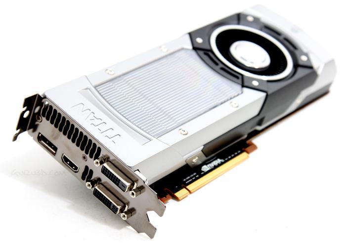
So then, it's time to talk business. The GeForce GTX Titan released today is based on the GK110 Kepler GPU architecture. The chip is huge in size, interestingly enough it is still based on the 28nm fabrication node.But when I say huge, I mean it as it has 7.1 Billion transistors tucked awau in a 45 mm × 45 mm 2397-pin S-FCBGA chip.
The GPU on that 10.5 inches long dual-slot GeForce GTX Titan graphics card boasts an impressive 2688 CUDA (shader) cores and has 7100 Million transistors. The product is obviously PCI-Express 3.0 ready and has a TDP of around 250W with a typical idle power draw of 15 Watts. That TDP is a maximum overall, and on average your GPU will not consume that amount of power. But let me first show you the GK110 GPU die:
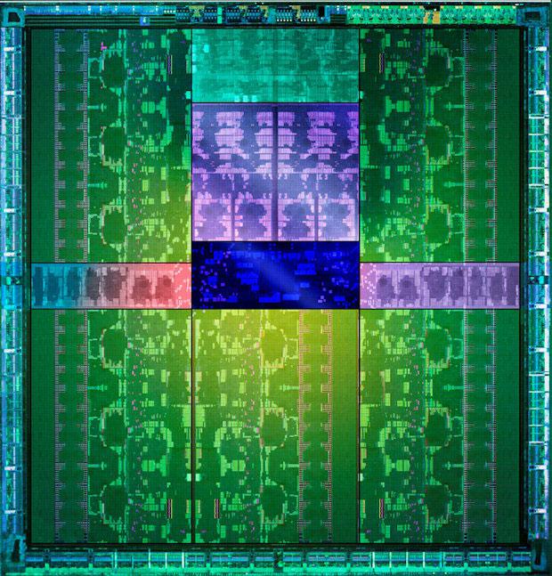
NVIDIA GK110 Kepler architecture GPU - you can see 15 sets of SMX clusters
The GK110 is based off the Kepler architecture, as such you will get the fairly standard pre-modelled SMX clusters of 192 shader processors per cluster. Out of the 15 available, there are 14 active SMX clusters for Titan, times 192 shader processors which thus offers you 2688 shader processors. If it would have had the full 15 SMX clusters enabled, yeah that would have been 2880 shader processors. There is a distinct difference with extra double precision units, but we'll talk about that on the next page though. But how does 4.5 Teraflops of peak compute performance sounds?
But to make a bold comparison, the mighty GeForce GTX 680 which many of you guys have have 1536 of these shader processors. We'll get more in-depth into the architecture on the next page though. As far as the memory specs of the GK110 Kepler GPU are concerned, the boards will feature a 384-bit memory bus connected to a near silly 6 GB of GDDR5 video buffer memory, aka VRAM aka your framebuffer aka graphics memory.
On the memory controller side of things you'll see that the reference memory clock (effective data-rate) is now set at 6 GHz / Gbps. This boils down to an exotic memory bandwidth of no less than 288 GB/s on that 384-bit memory bus. Much like the GTX 680, the GPU core versus the shader processor domain is are both clocked at 1:1, meaning both the core and shader domain clock in at a 836 MHz reference base clock frequency. One clock to rule them all (well internally there are dozens of different other clocks really, but let's keep it simple shall we?). With this release, NVIDIA now has the final series Kepler cards on their way. We expect at first launch wave to see maybe 10 maybe 20K cards available, so you'd better be fast if you want one. Obviously, later on there will be more batches available depending on demand. This is not going to be a 'limited' or extremely hard to get product series.
The new graphics adapters are of course DirectX 11.1 ready. With Windows 8, 7 and Vista also being DX11.1 ready with game compatibility to take advantage of DirectCompute, multi-threading, hardware tessellation and the latest shader 5.0 extensions. For your reference here's a quick overview of some past generation high-end GeForce cards opposed to the new Kepler based GeForce GTX 680.
| Single GPU based cards | GeForce GTX 285 |
GeForce GTX 480 |
GeForce GTX 580 |
GeForce GTX 680 |
GeForce GTX Titan |
| Stream (Shader) Processors | 240 | 480 | 512 | 1536 | 2688 |
| Core Clock (MHz) | 648 | 700 | 772 | 1006 | 836 |
| Shader Clock (MHz) | 1476 | 1400 | 1544 | - | - |
| Boost Clock | - | - | - | 1058 | 876 |
| Memory Clock (effective MHz) | 2400 | 3700 | 4000 | 6000 | 6000 |
| Memory amount | 1024 MB | 1536 | 1536 | 2048 | 6144 |
| Memory Interface | 512-bit | 384-bit | 384-bit | 256-bit | 384-bit |
| Memory Type | gDDR3 | gDDR5 | gDDR5 | gDDR5 | gDDR5 |
| HDCP | Yes | Yes | Yes | Yes | Yes |
| Two Dual link DVI | Yes | Yes | Yes | Yes | Yes |
| HDMI | No | Yes | Yes | Yes | Yes |
For Kepler overall, Nvidia kept their memory controllers GDDR5 compatible. Memory wise, Nvidia has nice large memory volumes available due to their architecture, we pass 2 GB as standard these days for most of Nvidia's series 600 graphics cards. The 6GB on the GTX Titan however is excessive, but with 6 memory controllers available, it would have been either 3 or 6 GB. The hardware engineers of Nvidia reworked the memory subs system quite a bit, enabling much higher memory clock frequency speeds compared to previous generation GeForce GPUs. The result is this memory speeds up-to 6 Gbps. Each memory partition utilizes one memory controller on the respective GPU, Titan has a total board memory of 6 GB and that's 24 pieces of 64M × 16 GDDR5, SDRAM.
- The GTX 580 has six memory controllers (6x256MB) = 1536 MB of GDDR5 memory
- The GTX 680 has four memory controllers (4x512MB) = 2048 MB of GDDR5 memory
- The GTX Titan has six memory controllers (6x1024MB) = 6144 MB of GDDR5 memory